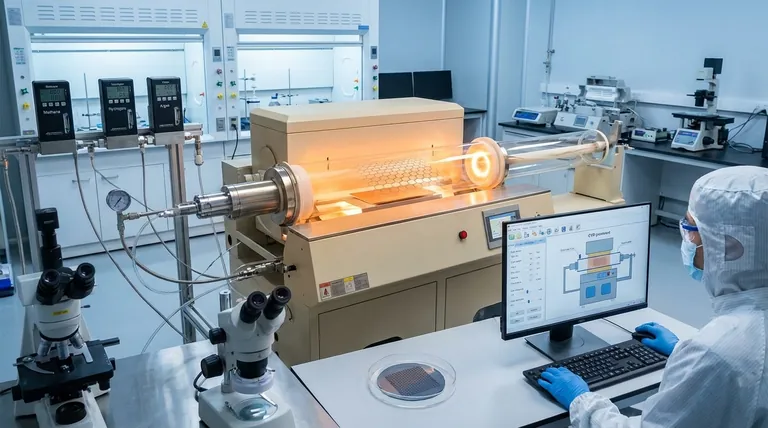
The most common method for synthesizing high-quality, large-area graphene is Chemical Vapor Deposition (CVD). This "bottom-up" approach effectively "grows" a one-atom-thick layer of carbon onto a metal substrate from a carbon-containing gas. It has become the industry standard for producing graphene suitable for commercial and electronic applications due to its scalability and the quality of the resulting film.
Chemical Vapor Deposition is less about creating graphene from a larger material and more about precisely assembling it, atom by atom, onto a surface. This control is what makes it invaluable for producing large, uniform sheets required for advanced electronics.
How the CVD Process Works
The elegance of CVD lies in its controlled, step-by-step process. It transforms simple gas molecules into a highly structured, two-dimensional crystal of graphene.
The Core Principle: Building from the Bottom Up
CVD is a bottom-up synthesis method. Instead of exfoliating or breaking down a large piece of graphite, it builds the graphene sheet from individual carbon atoms.
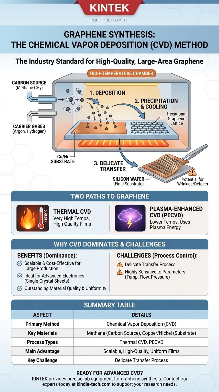
This is achieved by introducing a carbon source, typically a gas, into a high-temperature chamber containing a substrate material.
Key Ingredients for Growth
The process requires a specific set of materials to function correctly.
- Carbon Source: The most popular and effective carbon source is methane gas (CH4). Other sources like petroleum asphalt can be used but are more difficult to manage.
- Substrate: The graphene is grown on a metal foil substrate, which acts as a catalyst. Copper (Cu) and Nickel (Ni) are the most common choices.
- Carrier Gases: Inert gases like argon and reactive gases like hydrogen are used. They help control the reaction environment, improve the reaction rate, and ensure a clean deposition process.
The Growth Process Step-by-Step
At its core, the CVD process for graphene involves three main stages.
- Decomposition: At very high temperatures, the methane gas decomposes, breaking apart and releasing individual carbon atoms.
- Deposition: These free carbon atoms diffuse and deposit onto the surface of the hot metal foil.
- Precipitation & Cooling: As the chamber cools, the carbon atoms arrange themselves into the characteristic hexagonal lattice structure of graphene, forming a continuous, single-atom-thick film across the substrate.
After growth, the graphene sheet must be carefully transferred from the metal foil to a different substrate (like silicon) for use in electronic devices.
Two Paths to Graphene: Thermal vs. Plasma-Enhanced CVD
While the goal is the same, there are two primary variations of the CVD technique used for graphene synthesis.
Thermal CVD
This is the classic approach. It relies purely on very high temperatures (often around 1000°C) to decompose the carbon source gas and catalyze the reaction on the metal substrate. It is renowned for producing very high-quality graphene films.
Plasma-Enhanced CVD (PECVD)
This method uses plasma to energize the gas molecules. By creating a plasma, the chemical reactions can occur at much lower temperatures. This can be advantageous for certain applications and substrates that cannot withstand extreme heat.
Understanding the Trade-offs
While CVD is a powerful technique, it is not without its challenges. Understanding its limitations is key to appreciating its role in the industry.
The Challenge of Transfer
The graphene grown on the metal foil is rarely used there. It almost always needs to be transferred to a final substrate, such as a silicon wafer. This transfer process is delicate and can introduce wrinkles, tears, and impurities into the otherwise pristine graphene sheet, potentially degrading its exceptional electronic properties.
Process Control is Crucial
The final quality of the graphene film is highly sensitive to process parameters. Variables like temperature, gas flow rates, pressure, and cooling speed must be meticulously controlled. Any deviation can result in defects or the growth of multiple layers of graphene instead of a perfect monolayer.
Why CVD Dominates Graphene Production
CVD has emerged as the leading method because it uniquely addresses the core requirements for making graphene a viable commercial technology. It is a cost-effective and scalable process that delivers the quality needed for real-world applications.
- If your primary focus is advanced electronics: CVD is the only proven method for growing the large-area, single-crystal graphene sheets necessary for transistors and other high-performance components.
- If your primary focus is large-scale production: CVD is a highly scalable process, capable of producing large quantities of graphene film in a cost-effective manner compared to other methods.
- If your primary focus is material quality and uniformity: When properly controlled, CVD yields graphene with outstanding structural integrity and consistent electronic properties across a large area.
Ultimately, the Chemical Vapor Deposition process is the critical bridge taking graphene from a laboratory curiosity to a revolutionary industrial material.
Summary Table:
| Aspect | Details |
|---|---|
| Primary Method | Chemical Vapor Deposition (CVD) |
| Key Materials | Methane (Carbon Source), Copper/Nickel (Substrate) |
| Process Types | Thermal CVD, Plasma-Enhanced CVD (PECVD) |
| Main Advantage | Scalable production of high-quality, uniform graphene films |
| Key Challenge | Delicate transfer process from metal substrate to final application surface |
Ready to integrate high-quality graphene synthesis into your research or production line? KINTEK specializes in providing the precise lab equipment and consumables needed for advanced CVD processes. Whether you're developing next-generation electronics or scaling up material production, our expertise ensures you have the reliable tools for success. Contact our experts today to discuss how we can support your laboratory's specific graphene synthesis needs!
Visual Guide
Related Products
- Chemical Vapor Deposition CVD Equipment System Chamber Slide PECVD Tube Furnace with Liquid Gasifier PECVD Machine
- Customer Made Versatile CVD Tube Furnace Chemical Vapor Deposition Chamber System Equipment
- HFCVD Machine System Equipment for Drawing Die Nano-Diamond Coating
- Split Chamber CVD Tube Furnace with Vacuum Station Chemical Vapor Deposition System Equipment Machine
- Multi Heating Zones CVD Tube Furnace Machine Chemical Vapor Deposition Chamber System Equipment
People Also Ask
- What happens during deposition chemistry? Building Thin Films from Gaseous Precursors
- What is the chemical vapor deposition growth process? Build Superior Thin Films from the Atom Up
- Why is Chemical Vapor Deposition (CVD) equipment uniquely suited for constructing hierarchical superhydrophobic structures?
- What are the advantages of chemical vapor deposition? Achieve Superior Thin Films for Your Lab
- What types of substrates are used in CVD to facilitate graphene films? Optimize Graphene Growth with the Right Catalyst


