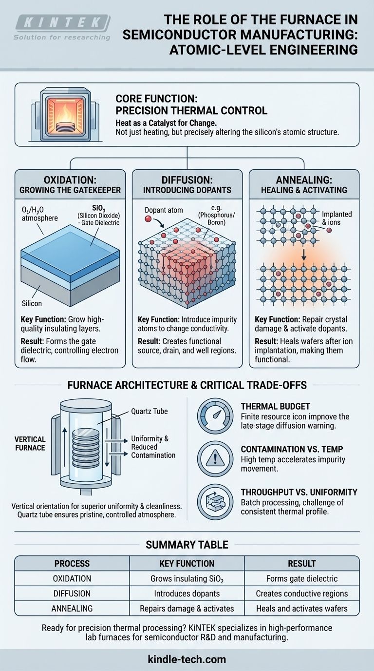
In semiconductor manufacturing, a furnace is a high-temperature processing chamber used to precisely modify the chemical and electrical properties of silicon wafers. These thermal processes are not simply about heating; they involve carefully controlled temperatures, gas atmospheres, and time durations to perform three critical functions: growing high-quality insulating layers (oxidation), introducing impurities to change conductivity (diffusion), and repairing crystal damage (annealing).
The core purpose of a furnace is not just to heat a wafer, but to use thermal energy as a tool to intentionally alter the silicon's atomic structure, enabling the creation of the fundamental building blocks of an integrated circuit.
The Core Function: Precision Thermal Control
A semiconductor furnace is far more than a simple oven. It is an instrument of atomic-level engineering where heat is the primary catalyst for change.
The entire process is governed by a precise recipe that dictates temperature ramps, stabilization times, gas compositions, and flow rates. Even minor deviations can compromise the performance and reliability of the final microchip.
Oxidation: Growing the Gatekeeper
The most fundamental furnace process is thermal oxidation. This involves heating a silicon wafer in an environment containing oxygen or water vapor.
This process causes a layer of silicon dioxide (SiO₂)—a highly stable and uniform insulator—to grow on the wafer's surface. This oxide layer is critical; it serves as the gate dielectric in a MOSFET transistor, the thin barrier that controls the flow of electrons. The quality and thickness of this layer directly determine the transistor's performance.
Diffusion: Introducing Dopants
To create functional transistors, specific regions of the silicon must have their electrical conductivity altered. This is achieved by introducing impurity atoms, known as dopants, into the silicon crystal lattice.
The furnace facilitates diffusion, where high temperatures provide the energy needed for dopant atoms (like phosphorus for n-type or boron for p-type) to move from the wafer's surface deep into the silicon. By controlling temperature and time, engineers can precisely define the depth and concentration of these doped regions, forming the source, drain, and well structures of a transistor.
Annealing: Healing and Activating
Processes like ion implantation, where dopants are physically shot into the wafer, cause significant damage to the silicon's crystal structure. The implanted atoms are also not initially in the correct lattice positions to be electrically active.
Annealing is a thermal process used to repair this damage. By heating the wafer to a specific temperature, the silicon atoms can rearrange themselves back into a stable crystal lattice. This same thermal energy also allows the implanted dopant atoms to move into the correct positions and become electrically "activated," making the doped region functional.
Understanding Furnace Architecture
Modern fabs primarily use two types of furnace systems, each designed to maximize control and minimize contamination.
Vertical vs. Horizontal Furnaces
While older fabs used horizontal furnaces where wafers were processed lying down, modern manufacturing overwhelmingly uses vertical furnaces. In a vertical furnace, wafers are stacked on top of each other in a quartz "boat."
This vertical orientation offers superior temperature uniformity across the wafers and significantly reduces the risk of particle contamination, as particles are more likely to fall to the bottom of the chamber rather than onto the wafer surfaces.
The Critical Role of the Quartz Tube
Wafers are not placed directly into the furnace itself. Instead, they are loaded into an ultra-pure quartz tube.
This tube isolates the wafers from the metallic heating elements and the outside environment, creating a pristine, controlled atmosphere. The purity of the quartz is paramount, as any contaminants leaching from the tube at high temperatures could diffuse into the silicon and ruin the devices.
The Critical Trade-offs
Using a furnace involves a delicate balance of competing factors. These trade-offs are central to the work of a process engineer.
Thermal Budget: A Finite Resource
Every high-temperature step consumes part of the wafer's thermal budget. This is the total amount of thermal processing a wafer can endure before previous steps are negatively affected.
For example, a late-stage annealing process can cause dopants from an earlier diffusion step to spread further than intended, blurring the edges of a transistor and altering its performance. Managing the thermal budget across dozens of steps is one of the most complex challenges in process integration.
Contamination vs. Temperature
High temperatures accelerate everything, including the movement of unwanted contaminants. A single metallic atom diffusing into the active region of a transistor can create a leakage path and cause the device to fail.
This forces an uncompromising focus on cleanliness, from the purity of the process gases to the material of the furnace tube and wafer handling equipment.
Throughput vs. Uniformity
Batch furnaces, which process 100-150 wafers at a time, offer high throughput, which is essential for cost-effective manufacturing. However, ensuring every single wafer in the batch experiences the exact same thermal profile is a significant engineering challenge.
Small temperature variations from the top to the bottom of the batch can lead to slight differences in oxide thickness or junction depth, impacting chip-to-chip consistency.
Making the Right Choice for Your Goal
Understanding furnace processes is key to connecting device physics with the realities of manufacturing.
- If your primary focus is process integration: Your chief concern is managing the cumulative thermal budget to ensure that each thermal step achieves its goal without disturbing the results of prior steps.
- If your primary focus is device physics: You must recognize that furnace oxidation and diffusion directly create the physical structures—the gate oxide and doped junctions—that govern transistor behavior and performance.
- If your primary focus is manufacturing yield: Your goal is to guarantee process uniformity and minimize contamination within the furnace to produce consistent, reliable devices across every wafer in every batch.
Ultimately, mastering the furnace is mastering the fundamental art of transforming pure silicon into a complex integrated circuit.
Summary Table:
| Process | Key Function | Result |
|---|---|---|
| Oxidation | Grows insulating silicon dioxide (SiO₂) layer | Forms the gate dielectric for transistors |
| Diffusion | Introduces dopant atoms to alter conductivity | Creates source, drain, and well regions |
| Annealing | Repairs crystal damage and activates dopants | Heals wafers after ion implantation |
Ready to achieve precision thermal processing in your lab? KINTEK specializes in high-performance lab furnaces and equipment designed for the exacting demands of semiconductor R&D and manufacturing. Our solutions deliver the temperature uniformity, contamination control, and reliability you need for oxidation, diffusion, and annealing processes. Contact our experts today via our Contact Form to discuss how we can support your semiconductor fabrication goals.
Visual Guide
Related Products
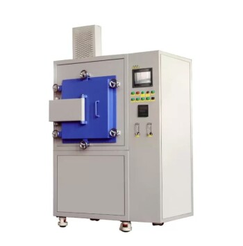
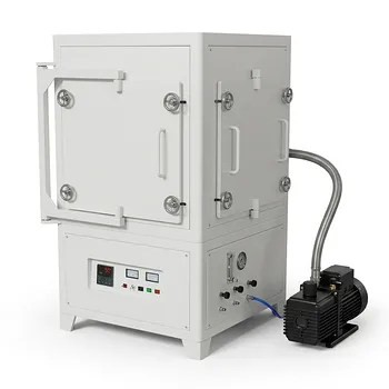
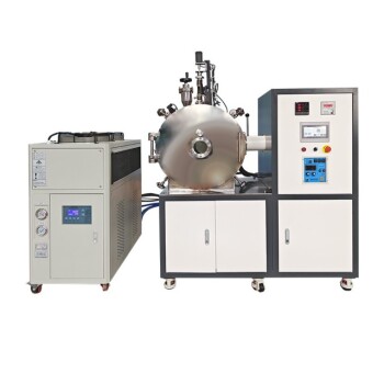
- Graphite Vacuum Furnace High Thermal Conductivity Film Graphitization Furnace
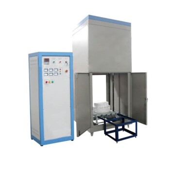
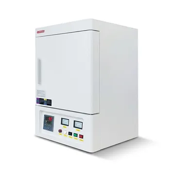
- High Temperature Muffle Oven Furnace for Laboratory Debinding and Pre Sintering
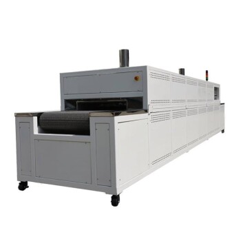
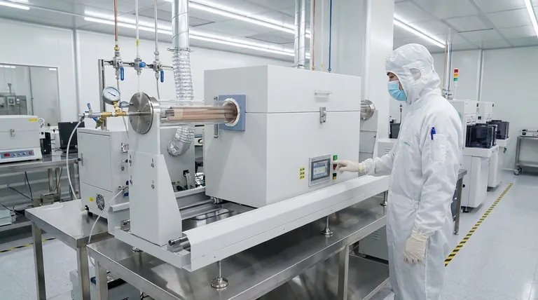
- Multi Heating Zones CVD Tube Furnace Machine Chemical Vapor Deposition Chamber System Equipment
- Mesh belt controlled atmosphere furnace
- Laboratory Muffle Oven Furnace Bottom Lifting Muffle Furnace
People Also Ask
- What are the interferences of graphite furnace? Overcome Matrix & Spectral Issues for Accurate GFAAS
- What is the use of graphite furnace? Achieve Extreme-Temperature Processing for Advanced Materials
- What are the advantages of graphite furnace over flame? Achieve Superior Trace Analysis Sensitivity
- What is the temperature range of a graphite furnace? Unlock up to 3000°C for advanced materials processing.
- What is the disadvantage of graphite furnace? Managing Reactivity and Contamination Risks