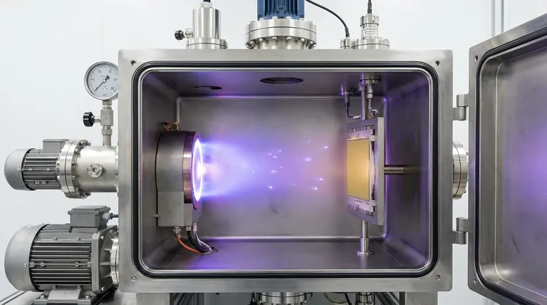
In essence, Physical Vapor Deposition (PVD) is a vacuum-based coating process that transforms a solid material into a vapor, which then travels and condenses onto a target object, or substrate, to form a high-performance thin film. The entire process occurs within a low-pressure chamber and is typically broken down into four distinct stages: vaporization of a source material, transportation of that vapor, reaction with other gases, and finally, deposition onto the substrate.
PVD is not a single technique but a family of processes sharing a common principle: manipulating materials atom-by-atom in a vacuum. By controlling how a material is vaporized and what it reacts with before landing on a surface, we can engineer coatings with precisely defined properties like extreme hardness, corrosion resistance, and unique colors.
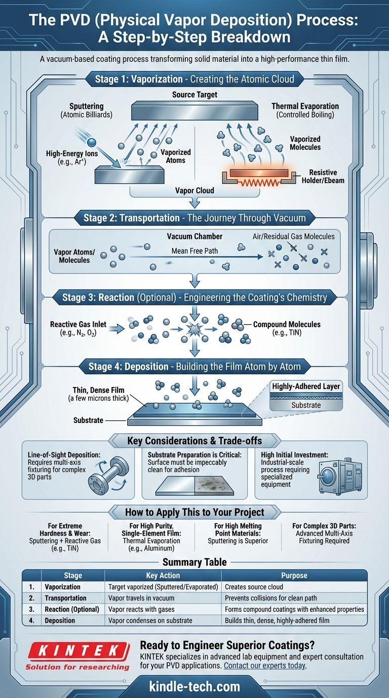
A Breakdown of the PVD Process
The PVD process is a sequence of carefully controlled physical events. While the specific parameters change based on the desired outcome, the fundamental stages remain constant across all PVD methods.
Step 1: Vaporization - Creating the Atomic Cloud
The process begins with the source material, known as the target, which is a solid block of the material to be deposited. This target is subjected to a high-energy source inside the vacuum chamber, causing atoms or molecules to be ejected from its surface and form a vapor.
The method of vaporization is the primary differentiator between PVD techniques.
Step 2: Transportation - The Journey Through Vacuum
Once vaporized, the atoms travel from the target to the substrate. This journey takes place in a vacuum to prevent the vaporized atoms from colliding with air or other residual gas molecules.
This "mean free path" is critical. Without a vacuum, the atoms would scatter, react uncontrollably, and fail to deposit a clean, dense film on the substrate.
Step 3: Reaction - Engineering the Coating's Chemistry
This stage is optional but provides much of PVD's versatility. A precisely controlled amount of a reactive gas, such as nitrogen, oxygen, or a hydrocarbon, is introduced into the chamber.
The vaporized metal atoms react with this gas mid-flight. For example, titanium vapor reacting with nitrogen gas forms the gold-colored, exceptionally hard titanium nitride (TiN) compound before it even reaches the surface. This allows for the creation of ceramic coatings like oxides, nitrides, and carbides from a pure metal source.
Step 4: Deposition - Building the Film Atom by Atom
Finally, the stream of vaporized atoms or newly formed compound molecules reaches the substrate. Because the substrate is typically at a lower temperature, the vapor condenses onto its surface.
This condensation builds a thin, highly-adhered film, often just a few microns thick. The atoms arrange themselves into a dense, hard layer that bonds tightly to the substrate material.
The Two Primary Methods of Vaporization
The method used in Step 1 defines the PVD process type and its best applications. The two most common methods are Sputtering and Thermal Evaporation.
Sputtering: Atomic Billiards
In sputtering, the target is bombarded with high-energy ions, usually from an inert gas like Argon. These ions act like atomic-scale cue balls, knocking atoms loose from the target material.
This method is highly controllable and is excellent for depositing alloys or materials with very high melting points that are difficult to evaporate.
Thermal Evaporation: Controlled Boiling
Thermal evaporation involves heating the source material in the vacuum until it evaporates (for liquids) or sublimates (for solids). This is often done by passing a current through a resistive holder or using a high-energy electron beam.
The resulting vapor then rises and condenses on the substrate. This method is generally simpler and faster for depositing pure metals with lower melting points, such as aluminum for reflective coatings.
Understanding the Trade-offs and Considerations
While powerful, PVD is not a universal solution. Understanding its limitations is key to successful implementation.
Line-of-Sight Deposition
PVD is a line-of-sight process. The vaporized atoms travel in a straight line from the source to the substrate. Any surface that is not in the direct path of the vapor stream will not be coated.
To coat complex 3D parts uniformly, sophisticated fixtures that rotate the substrate on multiple axes during deposition are required.
Substrate Preparation is Critical
The adhesion and quality of a PVD coating are entirely dependent on the cleanliness of the substrate. The surface must be impeccably clean, free from oils, oxides, and any other contaminants.
Failure to properly clean and prepare the substrate is the most common cause of coating failure, such as flaking or poor adhesion.
High Initial Investment
PVD equipment, including vacuum chambers, high-voltage power supplies, and high-capacity pumps, represents a significant capital investment. This makes it an industrial-scale process rather than a small-shop capability.
How to Apply This to Your Project
Your choice of PVD method and parameters should be driven by the end goal for your component.
- If your primary focus is extreme hardness and wear resistance: Sputtering combined with a reactive gas to form a ceramic like Titanium Nitride (TiN) or Titanium Aluminum Nitride (TiAlN) is the standard approach.
- If your primary focus is a highly pure, single-element film (e.g., aluminum for optics): Thermal evaporation is often a more straightforward and cost-effective method.
- If your primary focus is coating a material with a very high melting point: Sputtering is the superior choice, as it does not rely on melting the source material.
- If your primary focus is coating complex 3D parts: You must collaborate with a vendor that has advanced, multi-axis fixturing capabilities to ensure complete and uniform coverage.
By understanding these core principles, you can effectively determine how PVD can be leveraged to achieve your specific material performance goals.
Summary Table:
| Stage | Key Action | Purpose |
|---|---|---|
| 1. Vaporization | Target material is vaporized (sputtered or evaporated) | Creates a cloud of source atoms/molecules |
| 2. Transportation | Vapor travels through a vacuum | Prevents collisions for a clean, direct path to the substrate |
| 3. Reaction (Optional) | Vapor reacts with introduced gases (e.g., N₂) | Forms compound coatings (e.g., TiN) with enhanced properties |
| 4. Deposition | Vapor condenses onto the substrate | Builds a thin, dense, and highly-adhered functional film |
Ready to Engineer Superior Coatings for Your Components?
PVD is a powerful but complex process. Choosing the right method—sputtering for hard, wear-resistant ceramic coatings or thermal evaporation for pure metal films—is critical to your project's success. KINTEK specializes in providing the advanced lab equipment and expert consultation needed to perfect your PVD applications, from substrate preparation to final deposition.
Let's discuss how PVD can solve your specific material challenges. Contact our experts today to explore the ideal coating solution for your laboratory's needs.
Visual Guide
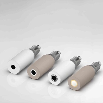
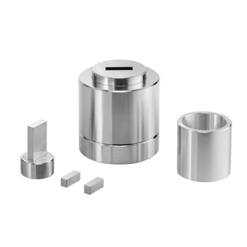
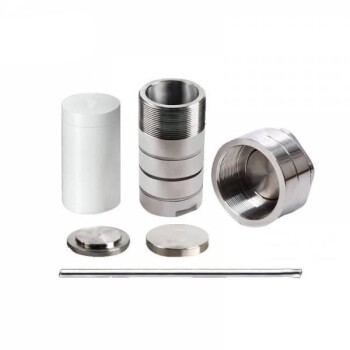
Related Products
- RF PECVD System Radio Frequency Plasma-Enhanced Chemical Vapor Deposition RF PECVD
- Inclined Rotary Plasma Enhanced Chemical Vapor Deposition PECVD Equipment Tube Furnace Machine
- Chemical Vapor Deposition CVD Equipment System Chamber Slide PECVD Tube Furnace with Liquid Gasifier PECVD Machine
- Microwave Plasma Chemical Vapor Deposition MPCVD Machine System Reactor for Lab and Diamond Growth
- VHP Sterilization Equipment Hydrogen Peroxide H2O2 Space Sterilizer
People Also Ask
- Why is PECVD environment friendly? Understanding the Eco-Friendly Benefits of Plasma-Enhanced Coating
- What are the advantages of PECVD? Enable Low-Temperature, High-Quality Thin-Film Deposition
- Why does PECVD commonly use RF power input? For Precise Low-Temperature Thin Film Deposition
- What are the benefits of PECVD? Achieve Superior Low-Temperature Thin Film Deposition
- What are the applications of PECVD? Essential for Semiconductors, MEMS, and Solar Cells