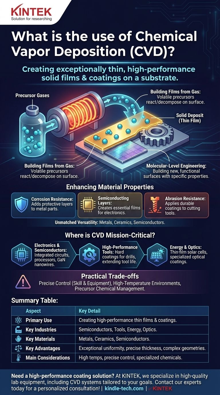
At its core, chemical vapor deposition (CVD) is used to create exceptionally thin, high-performance solid films and coatings on a substrate. This process is critical in numerous advanced manufacturing fields, including electronics for producing semiconductor devices, heavy industry for creating wear-resistant tool coatings, and energy for manufacturing thin-film solar cells. By depositing materials one layer of atoms at a time, CVD fundamentally enhances the properties of a base material.
The central purpose of chemical vapor deposition is to engineer a material's surface at the molecular level. It's not just about applying a layer; it's about building a new, functional surface with specific properties like electrical conductivity, hardness, or corrosion resistance that the original material lacks.
What Does Chemical Vapor Deposition Actually Do?
Building Films from Gas
Chemical vapor deposition is a process where a substrate (the object to be coated) is exposed to one or more volatile precursor gases. These gases react or decompose on the substrate's surface, leaving behind a solid deposit of the desired material.
This method allows for the creation of coatings with extremely precise thickness and uniformity.
Enhancing Material Properties
The primary goal of CVD is not just to coat an object, but to give its surface entirely new characteristics. The deposited films are engineered for specific functions.
This could mean adding corrosion resistance to a metal part, creating a semiconducting layer on a silicon wafer, or applying an abrasion-resistant coating to a cutting tool.
Unmatched Versatility
CVD can be used to deposit a vast range of materials, including various metals, ceramics, and semiconductors.
This versatility extends to the substrates being coated, which can include metals, glass, ceramics, and other materials capable of withstanding the process temperatures.
Where is CVD Mission-Critical?
Electronics and Semiconductors
The modern electronics industry is built on CVD. It is the go-to method for depositing the multiple thin films required to manufacture integrated circuits, processors, and memory chips.
It's also used to grow advanced materials like carbon nanotubes and gallium nitride (GaN) nanowires, which are essential for next-generation electronic and optoelectronic devices.
High-Performance Tools and Components
In industrial settings, CVD is used to apply hard, durable coatings to cutting tools, drills, and machine parts.
These coatings dramatically reduce wear and corrosion, extending the life and performance of tools used in high-stress environments like automotive and aerospace manufacturing.
Energy and Optics
The production of thin-film solar cells relies on CVD to deposit the photovoltaic materials that convert sunlight into electricity.
Beyond solar, it's used for creating specialized optical coatings for lenses, holographic displays, and other components where light management is critical.
Acknowledging the Practical Trade-offs
Requirement for Precise Control
CVD is not a simple process. Achieving a uniform, high-quality film requires precise control over temperature, pressure, gas flow rates, and chamber chemistry.
This complexity means that a high level of skill and sophisticated equipment are necessary for successful and repeatable results.
High-Temperature Environments
Many CVD processes require very high temperatures to initiate the necessary chemical reactions on the substrate's surface.
This can limit the types of substrate materials that can be used, as some may not be able to withstand the heat without deforming or melting.
Precursor Chemical Management
The "chemical" in CVD refers to the precursor gases, which can be expensive, toxic, or corrosive.
Proper handling, storage, and disposal of these chemicals are critical safety and operational considerations that add to the overall cost and complexity of the process.
Making the Right Choice for Your Goal
The decision to use CVD is driven by the need for a specific, high-performance surface property that cannot be achieved by other means.
- If your primary focus is producing the highest-purity semiconductor films: CVD is the industry standard for creating the foundational layers of microelectronics with unparalleled control.
- If your primary focus is adding extreme durability to industrial components: CVD provides a robust, chemically bonded coating ideal for protecting tools and parts in harsh environments.
- If your primary focus is uniformly coating complex, non-line-of-sight geometries: CVD's gas-phase nature allows it to deposit flawless films on intricate surfaces that other methods cannot reach.
Ultimately, chemical vapor deposition is the definitive process when you must fundamentally enhance a material's surface with a perfectly uniform, high-performance thin film.
Summary Table:
| Aspect | Key Detail |
|---|---|
| Primary Use | Creating high-performance thin films and coatings on a substrate. |
| Key Industries | Semiconductors, Industrial Tools, Energy (Solar), Optics. |
| Key Materials | Metals, Ceramics, Semiconductors (e.g., Silicon, Gallium Nitride). |
| Key Advantages | Exceptional uniformity, precise thickness control, ability to coat complex geometries. |
| Main Considerations | Requires high temperatures, precise process control, and specialized precursor chemicals. |
Need a high-performance coating solution for your lab or production line?
Chemical vapor deposition is a powerful technique for creating the precise, durable thin films required for advanced applications in semiconductors, industrial tools, and energy technology. Choosing the right equipment is critical for success.
At KINTEK, we specialize in high-quality lab equipment, including CVD systems tailored to your specific research and production goals. Our expertise helps laboratories and manufacturers achieve superior results with reliable, efficient coating processes.
Let's discuss how a CVD solution from KINTEK can enhance your materials' properties. Contact our experts today for a personalized consultation!
Visual Guide
Related Products
- Chemical Vapor Deposition CVD Equipment System Chamber Slide PECVD Tube Furnace with Liquid Gasifier PECVD Machine
- RF PECVD System Radio Frequency Plasma-Enhanced Chemical Vapor Deposition RF PECVD
- Microwave Plasma Chemical Vapor Deposition MPCVD Machine System Reactor for Lab and Diamond Growth
- Customer Made Versatile CVD Tube Furnace Chemical Vapor Deposition Chamber System Equipment
- 915MHz MPCVD Diamond Machine Microwave Plasma Chemical Vapor Deposition System Reactor
People Also Ask
- What are the core advantages of PE-CVD in OLED encapsulation? Protect Sensitive Layers with Low-Temp Film Deposition
- What is the chemical vapor deposition growth process? Build Superior Thin Films from the Atom Up
- What are the advantages of chemical vapor deposition? Achieve Superior Thin Films for Your Lab
- What are the processes of vapor phase deposition? Understand CVD vs. PVD for Superior Thin Films
- What is plasma enhanced chemical vapor deposition PECVD equipment? A Guide to Low-Temperature Thin Film Deposition


