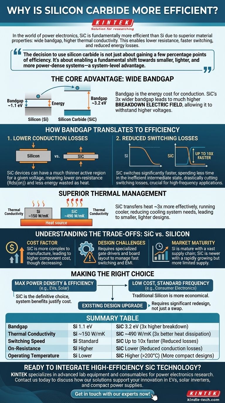
In the world of power electronics, silicon carbide (SiC) is fundamentally more efficient than traditional silicon (Si) because of its superior material properties. SiC's wide bandgap allows it to withstand higher voltages and temperatures, while its higher thermal conductivity lets it dissipate heat more effectively. These characteristics enable the creation of power devices that have lower electrical resistance and can switch on and off much faster, dramatically reducing the two primary sources of energy loss: conduction and switching losses.
The decision to use silicon carbide is not just about gaining a few percentage points of efficiency. It's about enabling a fundamental shift towards smaller, lighter, and more power-dense systems—a system-level advantage that often justifies its higher initial cost.
The Core Advantage: Understanding the Wide Bandgap
At the heart of SiC's superiority is a physical property called the bandgap. This determines the amount of energy required for an electron to jump from a non-conducting state to a conducting state.
What is a Bandgap?
Think of a bandgap as the "energy cost" to make a material conduct electricity. Materials with a low bandgap, like silicon, require less energy to become conductive. Materials with a high bandgap, like silicon carbide, require significantly more.
SiC's Bandgap Advantage Over Silicon
Silicon carbide has a bandgap of approximately 3.2 electron volts (eV), nearly three times that of silicon's 1.1 eV. This seemingly small difference has massive implications for performance. A wider bandgap directly leads to a much higher breakdown electric field.
This means SiC can withstand a much stronger electric field before it breaks down and current flows uncontrollably. This single property is the catalyst for most of SiC's other benefits.
How the Bandgap Translates to Efficiency
The higher breakdown field of SiC allows engineers to design power devices that are fundamentally better at their job—managing the flow of power with minimal waste.
Lower Conduction Losses
To handle a specific voltage, a SiC device can be made with a much thinner active region than a comparable silicon device.
A thinner path for electricity means lower electrical resistance, known as on-resistance (Rds(on)). According to the formula for power loss (P = I²R), lower resistance directly translates to less energy wasted as heat when the device is on. This is a reduction in conduction loss.
Reduced Switching Losses
Power devices waste significant energy during the transition from the "off" state to the "on" state and back. SiC devices can make this transition up to 10 times faster than silicon devices.
By spending less time in this inefficient intermediate state, SiC devices drastically cut down on switching losses. This advantage is especially critical in high-frequency applications like EV chargers and solar inverters, where the device switches thousands of times per second.
Superior Thermal Management
Efficiency is not just about reducing electrical loss; it's also about managing the heat that is inevitably generated. SiC has a thermal conductivity roughly three times higher than silicon.
This means it can transfer heat away from the device junction much more effectively. Better heat dissipation allows the device to run cooler, which improves its reliability and reduces the need for large, heavy, and expensive cooling systems like heatsinks and fans. This leads to smaller, lighter, and more power-dense final products.
Understanding the Trade-offs: SiC vs. Silicon
While SiC offers compelling advantages, it is not a universal replacement for silicon. The choice involves clear trade-offs that are critical to understand.
The Cost Factor
The primary barrier to SiC adoption is cost. Manufacturing high-quality SiC crystals (boules) is more complex and energy-intensive than producing silicon wafers. This results in a higher per-component cost, though this is steadily decreasing as the technology matures.
Design and Implementation Challenges
You cannot simply drop a SiC MOSFET into a circuit designed for a silicon MOSFET. The extremely fast switching speeds of SiC can create new problems, such as electromagnetic interference (EMI) and voltage overshoots.
Engineers must use specialized gate drivers designed to control SiC's unique characteristics and must pay careful attention to the board layout to manage these high-speed effects.
Market Maturity and Supply
Silicon has been the foundation of the electronics industry for over 50 years. Its manufacturing processes are incredibly refined, and the supply chain is vast and stable. SiC is a newer technology with a more limited, though rapidly growing, supply chain.
Making the Right Choice for Your Application
The decision between silicon and silicon carbide hinges entirely on your system-level goals.
- If your primary focus is maximum power density and efficiency (e.g., EVs, solar inverters, high-end server power supplies): SiC is the definitive choice, as its system-level benefits in size, weight, and cooling reduction justify the higher component cost.
- If your primary focus is low cost in standard-frequency applications (e.g., most consumer electronics, basic industrial power): Traditional silicon remains the more economical and practical solution for now.
- If you are considering an upgrade to an existing design: A move to SiC requires a significant redesign effort for the gate driver circuit and board layout, not just a component swap.
Ultimately, choosing the right material requires weighing component cost against the profound system-wide benefits that greater efficiency enables.
Summary Table:
| Feature | Silicon (Si) | Silicon Carbide (SiC) | Advantage |
|---|---|---|---|
| Bandgap | 1.1 eV | 3.2 eV | 3x higher breakdown voltage |
| Thermal Conductivity | ~150 W/mK | ~490 W/mK | 3x better heat dissipation |
| Switching Speed | Standard | Up to 10x faster | Drastically reduced switching losses |
| On-Resistance | Higher | Lower | Reduced conduction losses |
| Operating Temperature | Lower | Higher (>200°C) | Enables more compact designs |
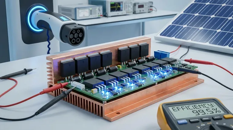
Ready to integrate high-efficiency silicon carbide technology into your lab's power electronics projects?
KINTEK specializes in providing advanced lab equipment and consumables for researchers and engineers pushing the boundaries of power electronics. Whether you're developing next-generation EV chargers, solar inverters, or compact power supplies, our expertise and product range can support your innovation.
Contact us today to discuss how our solutions can help you achieve superior performance and power density with SiC technology.
Get in touch with our experts now!
Visual Guide
Related Products
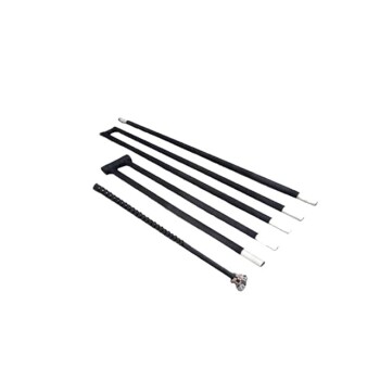
- Silicon Carbide (SIC) Ceramic Sheet Wear-Resistant Engineering Advanced Fine Ceramics
- Silicon Carbide (SIC) Ceramic Sheet Flat Corrugated Heat Sink for Engineering Advanced Fine Ceramics
- Silicon Carbide (SIC) Ceramic Plate for Engineering Advanced Fine Ceramics
- Silicon Carbide SiC Thermal Heating Elements for Electric Furnace
- Precision Machined Silicon Nitride (SiN) Ceramic Sheet for Engineering Advanced Fine Ceramics
People Also Ask
- What are the common uses of silicon carbide? Unlock Extreme Performance in Harsh Environments
- What is the strongest ceramics? Silicon Carbide Leads in Hardness & Thermal Strength
- What are the properties of SiC? Unlock High-Temperature, High-Frequency Performance
- What are the properties and applications of silicon carbide ceramics? Solve Extreme Engineering Challenges
- What is the temperature resistance of silicon carbide? Withstands Extreme Heat Up to 1500°C