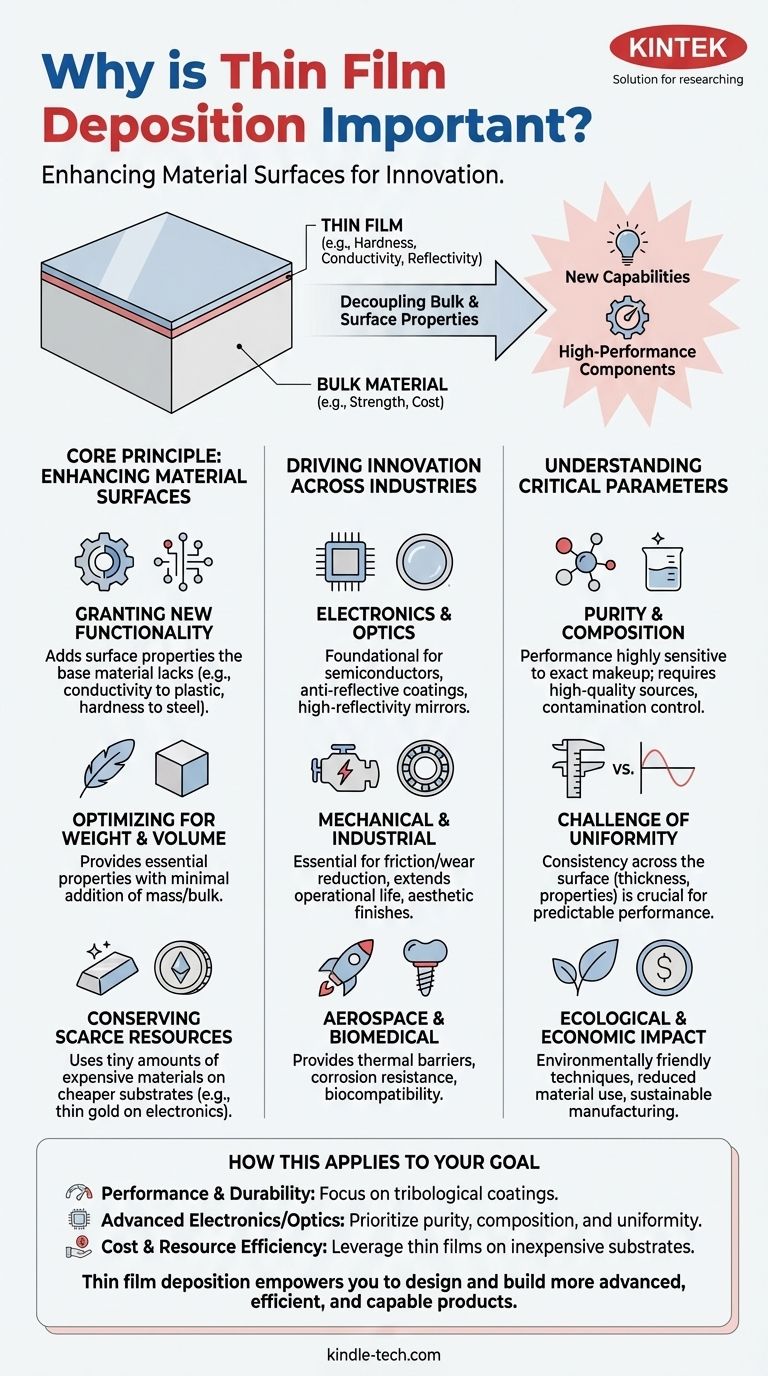
Thin film deposition is a cornerstone of modern technology because it allows us to fundamentally change the surface properties of a material. By applying an ultra-thin layer of a different substance, we can grant an object new capabilities—like electrical conductivity, wear resistance, or specific optical behaviors—that its bulk material does not possess. This enables the creation of entirely new products, improves the performance and longevity of existing ones, and conserves scarce resources.
The true importance of thin film deposition lies in its ability to separate a material's bulk properties (like strength and cost) from its surface properties (like hardness or reflectivity). This decoupling allows engineers to create high-performance, cost-effective components that would otherwise be impossible to manufacture.
The Core Principle: Enhancing Material Surfaces
At its heart, thin film deposition is about precision engineering at a microscopic scale. It solves the problem of needing a material to have contradictory properties, such as being both flexible and scratch-resistant, or inexpensive yet highly conductive.
Granting New Functionality
Many engineering challenges are solved by adding a surface property that the base material lacks. A thin film can make a plastic substrate electrically conductive or a steel tool incredibly hard and low-friction.
This process exposes a target material to an energized environment of gas, plasma, or liquid, which deposits the desired coating. The result is a composite material that combines the best attributes of the substrate and the film.
Optimizing for Weight and Volume
In fields like aerospace and electronics, every gram and cubic millimeter matters. Thin film deposition provides essential surface properties with minimal addition of volume and weight.
This is far more efficient than making the entire component out of a specialized, heavy, or expensive material.
Conserving Scarce or Expensive Materials
Thin films make it possible to use a tiny amount of a rare or costly material to impart its properties to a much larger, cheaper substrate.
For example, a thin layer of gold can provide excellent conductivity and corrosion resistance on an electronic component without the prohibitive cost of making the entire part from solid gold.
Driving Innovation Across Industries
The widespread impact of thin film deposition is evident in its vast range of applications. It is not an isolated technology but a foundational process that enables advances in nearly every major technical field.
In Electronics and Optics
The entire semiconductor industry is built upon thin film deposition. The process is used to create the intricate layers of conductive, insulating, and semiconducting materials that form microchips.
It is also critical for manufacturing high-performance optics, such as anti-reflective coatings on lenses and high-reflectivity mirrors.
In Mechanical and Industrial Applications
Thin films are essential for improving the tribological behavior of components—that is, their friction and wear characteristics. Hard, slick coatings on cutting tools, engine parts, and bearings dramatically extend their operational life.
This technology is also used for aesthetic purposes, providing durable, colored finishes on everything from watches to architectural fixtures.
In Aerospace and Biomedical Fields
In aerospace, thin films provide thermal barriers and corrosion resistance for components exposed to extreme environments.
In the biomedical field, specialized coatings make medical implants biocompatible, preventing the body from rejecting them and improving patient outcomes.
Understanding the Critical Parameters
The power of thin film deposition comes from extreme precision, and failure to control the process results in a useless product. The value of the technology is directly tied to the ability to manage its key variables.
The Demand for Purity and Composition
The performance of a thin film is highly sensitive to its exact chemical makeup. Unintentional impurities or slight variations in composition can drastically alter its electrical, optical, or mechanical properties.
Achieving the desired film requires high-quality source materials and precise control over the deposition environment to prevent contamination.
The Challenge of Uniformity
Uniformity refers to the consistency of the film across the entire surface of the substrate. This most often relates to thickness, but it can also apply to properties like the index of refraction or electrical resistance.
If a film is not uniform, its performance will be unpredictable. For example, a non-uniform optical coating will cause visual distortion, while a non-uniform conductive layer in a microchip will cause it to fail.
The Ecological and Economic Impact
Modern deposition techniques are often designed to be more environmentally friendly than older plating methods. They can lead to reduced effluent output and lower power consumption.
By extending the life of products and enabling the use of less material, thin film deposition contributes to a more sustainable and economically efficient manufacturing landscape.
How This Applies to Your Engineering Goal
Your specific application will determine which aspects of thin film deposition are most critical.
- If your primary focus is performance and durability: You will benefit most from tribological coatings that enhance hardness and reduce friction on mechanical parts.
- If your primary focus is advanced electronics or optics: Your success will depend on achieving exceptional purity, composition control, and uniformity for electrical and optical layers.
- If your primary focus is cost and resource efficiency: You should leverage thin films to apply the properties of expensive materials onto inexpensive, abundant substrates.
Ultimately, understanding thin film deposition empowers you to design and build more advanced, efficient, and capable products.
Summary Table:
| Key Benefit | Description |
|---|---|
| New Functionality | Adds properties like conductivity or hardness that the base material lacks. |
| Weight/Volume Optimization | Provides essential surface properties with minimal added mass or bulk. |
| Resource Conservation | Uses tiny amounts of expensive/rare materials on cheaper substrates. |
| Drives Innovation | Foundational process for semiconductors, optics, aerospace, and biomedical devices. |
| Critical Parameters | Success depends on precise control of purity, composition, and uniformity. |
Ready to enhance your product's performance with precision thin film deposition? KINTEK specializes in providing the advanced lab equipment and consumables necessary for achieving the high-purity, uniform coatings required in electronics, optics, and industrial applications. Our expertise can help you solve material challenges, improve product longevity, and use resources more efficiently. Contact our experts today to discuss how we can support your specific engineering goals.
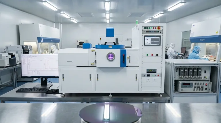
Visual Guide
Related Products
- Aluminized Ceramic Evaporation Boat for Thin Film Deposition
- Tungsten Evaporation Boat for Thin Film Deposition
- Electron Beam Evaporation Coating Oxygen-Free Copper Crucible and Evaporation Boat
- Molybdenum Tungsten Tantalum Evaporation Boat for High Temperature Applications
- Vacuum Hot Press Furnace Machine for Lamination and Heating
People Also Ask
- What are the alternatives to sputtering? Choose the Right Thin Film Deposition Method
- Why is an alumina boat selected for catalyst precursors? Ensure Sample Purity at 1000 °C
- What are thin films deposited by evaporation? A Guide to High-Purity Coating
- Why are high-purity ceramic boats used for lignin activation? Ensure Purity & Thermal Stability
- What is thin film deposition? Unlock Advanced Surface Engineering for Your Materials


