Introduction to Coating Methods
Types of Coating Methods
Coating methods for growing single crystal films encompass a spectrum of techniques, each with its unique mechanisms and applications. The primary methods include Chemical Vapor Deposition (CVD), Physical Vapor Deposition (PVD), and Epitaxy. These methods are not only diverse in their operational principles but also offer a range of sub-types and specific techniques tailored to various scientific and industrial needs.
-
Chemical Vapor Deposition (CVD) involves the chemical reaction of precursor gases to deposit a solid film on a substrate. This method includes sub-types such as Low-Pressure CVD (LPCVD), Atmospheric-Pressure CVD (APCVD), Plasma-Enhanced CVD (PECVD), and more. Each sub-type is optimized for specific conditions, allowing for precise control over film properties.
-
Physical Vapor Deposition (PVD), on the other hand, relies on the physical evaporation or sputtering of material to deposit it on a substrate. Sub-types within PVD include Electron beam evaporation, magnetron sputtering, and Pulsed Laser Deposition (PLD). These techniques are particularly useful for creating thin, uniform films with high purity.
-
Epitaxy methods, such as Molecular Beam Epitaxy (MBE), Vapor Phase Epitaxy (VPE), and Liquid Phase Epitaxy (LPE), focus on the growth of a single crystal film on a single crystal substrate. These methods are crucial for achieving high-quality, single-crystal structures, which are essential for advanced semiconductor applications.
Each of these methods has its own set of advantages and limitations, making them suitable for different applications. For instance, while CVD and PVD are versatile and widely used, epitaxy offers superior control over crystal structure and orientation, making it ideal for specialized applications in electronics and photonics.
Chemical Vapor Deposition (CVD)
Sub-types of CVD
Chemical Vapor Deposition (CVD) encompasses a diverse array of techniques, each tailored to specific applications and material properties. The primary methods include Low-Pressure Chemical Vapor Deposition (LPCVD), Atmospheric-Pressure Chemical Vapor Deposition (APCVD), Substrate-Assisted Chemical Vapor Deposition (SACVD), Plasma-Enhanced Chemical Vapor Deposition (PECVD), High-Density Plasma Chemical Vapor Deposition (HDPCVD), Flow-Conditioned Chemical Vapor Deposition (FCVD), and Metal-Organic Chemical Vapor Deposition (MOCVD).
These techniques fundamentally rely on the chemical reaction of precursor gases to deposit a solid film onto a substrate. The choice of method often hinges on factors such as deposition rate, film uniformity, and the desired material properties. For instance, LPCVD is renowned for its high-quality, uniform films, making it ideal for semiconductor manufacturing, while PECVD, leveraging plasma, can deposit films at lower temperatures, which is crucial for temperature-sensitive substrates.
| CVD Method | Key Characteristics | Typical Applications |
|---|---|---|
| LPCVD | High uniformity, low pressure | Semiconductor devices |
| APCVD | Operates at atmospheric pressure | Coating large substrates |
| SACVD | Enhanced by substrate properties | Advanced semiconductor structures |
| PECVD | Lower deposition temperature, uses plasma | Temperature-sensitive materials |
| HDPCVD | High plasma density, high deposition rate | High-performance coatings |
| FCVD | Flow control for precise deposition | Precision coatings |
| MOCVD | Uses metal-organic precursors | Optoelectronic devices |
Each sub-type of CVD offers unique advantages and challenges, making them suitable for different stages of material development and production. Understanding these nuances is essential for optimizing the growth of single crystal films and other advanced materials.
Physical Vapor Deposition (PVD)
Sub-types of PVD
Physical Vapor Deposition (PVD) encompasses a variety of techniques, each with its unique mechanisms and applications. Electron beam evaporation is one such method, where a high-energy electron beam is directed at a source material, causing it to evaporate and subsequently deposit onto a substrate. This technique is particularly useful for materials with high melting points and is often employed in the production of optical coatings.
Another prominent sub-type is magnetron sputtering, which involves the use of a magnetic field to enhance the ionization of target atoms. This method is highly efficient and is widely used in the semiconductor industry for depositing thin films with precise control over composition and thickness.
Pulsed Laser Deposition (PLD) stands out due to its ability to deposit complex oxide materials with high precision. In PLD, a high-energy laser pulse is directed at a target material, creating a plasma plume that deposits onto the substrate. This technique is favored for its ability to reproduce the target material's composition with minimal impurities.
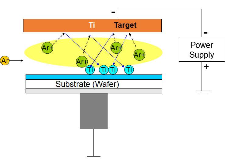
These methods, along with others like ion beam deposition and thermal evaporation, all share the common goal of physically transferring material from a source to a substrate to form a thin film. The choice of method often depends on the specific requirements of the application, such as film uniformity, adhesion, and the desired material properties.
Epitaxy
Sub-types of Epitaxy
Epitaxy encompasses a variety of specialized techniques designed to grow single crystal films on single crystal substrates. The primary methods include Molecular Beam Epitaxy (MBE), Vapor Phase Epitaxy (VPE), Liquid Phase Epitaxy (LPE), and Solid Phase Epitaxy (SPE). Each of these sub-types has unique characteristics and applications, making them suitable for different materials and growth conditions.
Molecular Beam Epitaxy (MBE) is a sophisticated technique that involves the deposition of material onto a heated substrate in a high vacuum environment. This method allows for precise control over the composition and thickness of the deposited layers, making it ideal for creating complex structures such as quantum wells and superlattices.
Vapor Phase Epitaxy (VPE), on the other hand, utilizes chemical reactions in the vapor phase to deposit the desired material onto the substrate. This technique is particularly useful for growing semiconductors and can be performed under various conditions, including atmospheric pressure and reduced pressure.
Liquid Phase Epitaxy (LPE) involves the growth of crystals from a saturated solution, where the substrate is immersed in a melt containing the desired material. This method is often used for producing high-quality single crystal films of materials such as gallium arsenide and indium phosphide.
Solid Phase Epitaxy (SPE) is a unique method where the growth occurs through the solid-state diffusion of atoms into the substrate. This technique is commonly used for recrystallization processes and is particularly effective for materials that are difficult to grow using other epitaxial methods.
Each of these epitaxial techniques plays a crucial role in the fabrication of advanced electronic and optoelectronic devices, contributing to the continuous advancement of semiconductor technology.
Film Formation Mechanisms
2D Layer-by-Layer Growth Mode
In the 2D layer-by-layer growth mode, the film develops in a highly structured and orderly manner, with each layer being meticulously completed before the subsequent layer begins its formation. This methodical process ensures that the film's surface remains exceptionally flat, a characteristic that is particularly advantageous for the cultivation of single crystal structures.
The meticulous nature of this growth mode is further highlighted by the controlled deposition process, where each atomic layer adheres precisely to the previous one, creating a seamless and uniform film. This precision is crucial for maintaining the structural integrity and crystalline quality of the film, making it an ideal choice for applications requiring high-purity single crystal materials.
Moreover, the flatness achieved through this method not only enhances the optical and electronic properties of the film but also facilitates easier integration with other semiconductor components. The controlled environment and precise deposition techniques employed in this mode allow for the fabrication of films with minimal defects and optimal performance, meeting the stringent requirements of advanced semiconductor technologies.
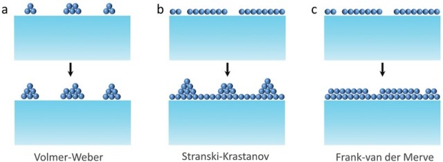
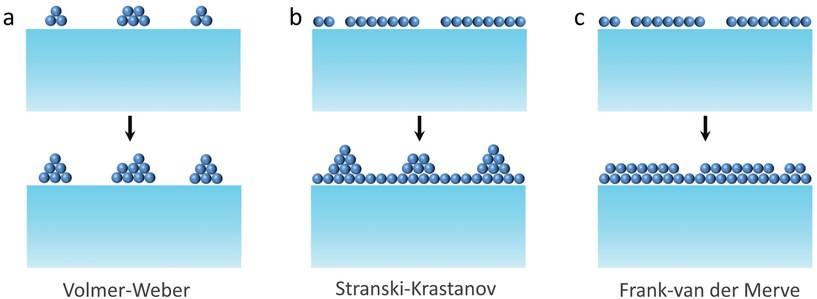
3D Island Growth (Volmer-Weber)
In the 3D Island Growth mode, also known as the Volmer-Weber mechanism, the film develops in localized, three-dimensional clusters or islands. Unlike the 2D Layer-by-Layer Growth mode, where the film expands uniformly across the substrate, the Volmer-Weber process results in discrete growth regions that eventually coalesce to cover the entire surface.
This island-based growth pattern arises due to the weak adhesion between the deposited material and the substrate. The lack of strong bonding forces allows the material to form distinct islands rather than spreading out uniformly. Consequently, the resulting film exhibits high surface free energy, which is indicative of an unstable and reactive surface.
The weak interaction between the film and the substrate can lead to several challenges. For instance, the film may exhibit poor mechanical adhesion, making it more susceptible to delamination or cracking. Additionally, the high surface free energy can contribute to increased reactivity, which might be undesirable in certain applications where stability and durability are critical.
To illustrate, consider a deposition process where the material forms islands rather than a continuous layer. This can be visualized as small mounds of material scattered across the surface, each mound representing a separate growth event. As more material is deposited, these mounds grow and eventually merge, forming a continuous but structurally weak film.
| Characteristic | Description |
|---|---|
| Growth Pattern | Island-based, 3D clusters |
| Adhesion | Weak interaction with substrate |
| Surface Energy | High surface free energy |
| Challenges | Poor mechanical adhesion, susceptibility to delamination |
In summary, the Volmer-Weber growth mode presents a unique challenge in film formation, characterized by localized island growth and high surface free energy. While this mode can cover the entire substrate, the resulting film's structural integrity and stability are compromised due to the weak substrate interaction.
Mixed-Mode Growth
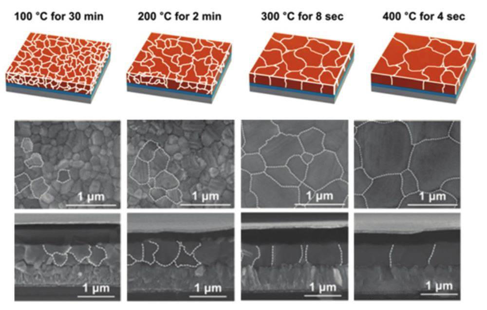
Mixed-Mode Growth represents a dynamic transition phase in the formation of single crystal films, where the initial stages of layer-by-layer growth gradually give way to the formation of islands. This hybrid growth mechanism is primarily driven by the accumulation of stress within the film, which disrupts the orderly progression of monolayer deposition.
Key Phases of Mixed-Mode Growth
-
Initial Layer-by-Layer Growth:
- During the initial phase, the film grows in a controlled, layer-by-layer manner, similar to the 2D growth mode. This phase is characterized by the complete coverage of each atomic layer before the next begins, ensuring a smooth and uniform surface.
- Techniques such as Molecular Beam Epitaxy (MBE) and Vapor Phase Epitaxy (VPE) are particularly adept at facilitating this initial layer-by-layer growth due to their precise control over the deposition process.
-
Transition to Island Formation:
- As the film continues to grow, internal stresses begin to accumulate, primarily due to mismatches in lattice constants between the film and the substrate. These stresses can arise from thermal expansion differences, chemical interactions, or mechanical strain.
- The accumulated stress eventually leads to the disruption of the continuous layer-by-layer growth, causing the film to transition into a 3D island growth mode. This transition is often referred to as the Volmer-Weber growth mode, where localized regions of the film grow independently as islands.
Structural Characteristics
- Mixed Structure: The resulting film exhibits a complex structure that combines elements of both 2D and 3D growth modes. The lower layers maintain the ordered, flat structure of layer-by-layer growth, while the upper layers are characterized by the presence of islands.
- Stress Distribution: The mixed-mode structure helps in redistributing the accumulated stress, preventing catastrophic failure of the film. The islands act as stress relief points, allowing the film to accommodate the mismatches without fracturing.
Implications for Film Properties
- Surface Roughness: The transition from 2D to 3D growth introduces surface roughness, which can affect the optical, electrical, and mechanical properties of the film.
- Adhesion and Cohesion: The mixed structure can lead to variations in adhesion and cohesion between the film and the substrate, impacting the overall stability and performance of the coating.
In summary, Mixed-Mode Growth is a critical phase in the formation of single crystal films, where the interplay between layer-by-layer deposition and island formation results in a unique structural morphology that balances stress and promotes film integrity.
Conclusion
Preferred Methods for Single Crystal Growth
Epitaxy methods, such as Molecular Beam Epitaxy (MBE), Vapor Phase Epitaxy (VPE), Liquid Phase Epitaxy (LPE), and Solid Phase Epitaxy (SPE), are particularly favored for producing single crystal films due to their distinctive 2D layer-by-layer growth mode. This methodical approach ensures that each atomic layer is meticulously deposited and aligned, fostering the formation of a highly ordered and continuous crystal structure.
In contrast, Chemical Vapor Deposition (CVD) and Physical Vapor Deposition (PVD) techniques often yield polycrystalline or amorphous films, unless stringent process conditions are meticulously maintained. The variability in these methods arises from their inherent deposition mechanisms, which can lead to the formation of multiple crystal orientations or non-crystalline structures if not carefully controlled.
| Method | Growth Mode | Typical Outcome |
|---|---|---|
| Epitaxy | 2D Layer-by-Layer | Single Crystal Films |
| CVD | Variable (2D/3D) | Polycrystalline or Amorphous Films |
| PVD | Variable (2D/3D) | Polycrystalline or Amorphous Films |
The table above highlights the primary differences in growth modes and typical outcomes for each method, underscoring the critical role of growth mode in determining the crystalline quality of the deposited films.
Related Products
- CVD Diamond Dressing Tools for Precision Applications
- Multi Heating Zones CVD Tube Furnace Machine Chemical Vapor Deposition Chamber System Equipment
- CVD Diamond Domes for Industrial and Scientific Applications
- CVD Diamond for Thermal Management Applications
- Chemical Vapor Deposition CVD Equipment System Chamber Slide PECVD Tube Furnace with Liquid Gasifier PECVD Machine
Related Articles
- Market Prospects and Applications of CVD Diamonds
- Preparation and Transfer Technology of Graphene by Chemical Vapor Deposition
- Comprehensive Overview of Chemical Vapor Deposition (CVD) Technologies
- CVD Diamond: Superior Material for Optical Windows
- Advantages and Disadvantages of Chemical Vapor Deposition (CVD)


