Introduction to Precision Ceramics in Semiconductors
Advantages of Ceramics in Semiconductor Equipment
Ceramics stand out as the material of choice for numerous components in semiconductor equipment, largely due to their exceptional mechanical and thermal properties. High hardness and high modulus of elasticity enable ceramics to withstand the extreme conditions and mechanical stresses encountered in semiconductor manufacturing. This ensures that the equipment operates reliably and with minimal wear, thereby reducing maintenance costs and downtime.
Moreover, the high wear resistance of ceramics is crucial in environments where friction and abrasion are common, such as in wafer polishers and etching equipment. This property extends the lifespan of critical components, contributing to the overall efficiency and longevity of the semiconductor manufacturing process.
Ceramics also excel in high insulation and corrosion resistance, which are essential for maintaining the integrity and performance of semiconductor equipment. The low thermal expansion coefficient of ceramics further enhances their suitability for precision applications, ensuring that dimensional stability is maintained even under varying thermal conditions.
In summary, the combination of high hardness, high modulus of elasticity, high wear resistance, high insulation, corrosion resistance, and low expansion makes ceramics indispensable for various parts in semiconductor equipment, ensuring optimal performance and reliability in the demanding semiconductor manufacturing environment.
Value of Precision Ceramics in Semiconductor Equipment
Precision ceramics play a pivotal role in the semiconductor industry, constituting approximately 16% of the total value of semiconductor equipment. These advanced materials are integral to a variety of critical processes within semiconductor manufacturing, ensuring high precision and reliability.
Precision ceramics are extensively utilized in silicon wafer polishers, where their hardness and wear resistance are crucial for achieving the smooth surfaces required for semiconductor devices. In vacuum heat treatment equipment, these ceramics provide excellent thermal stability, enabling consistent and controlled heating processes.
In photolithography, precision ceramics are employed in the intricate components that handle and manipulate photoresist-coated wafers, ensuring the high-resolution patterns necessary for semiconductor fabrication. Deposition equipment benefits from the low thermal expansion and high insulation properties of ceramics, which are essential for maintaining the precise conditions required for film deposition.
Etching equipment relies on precision ceramics for components that withstand harsh chemical environments and high temperatures, ensuring the precise removal of material layers. Ion implantation machines, which require materials that can handle high-energy particle beams without degradation, also utilize precision ceramics for their superior durability and resistance to radiation damage.
| Application Area | Ceramic Component Usage |
|---|---|
| Silicon Wafer Polishers | Hardness and wear resistance for smooth wafer surfaces |
| Heat Treatment Equipment | Thermal stability for consistent heating processes |
| Photolithography | Handling and manipulation of photoresist-coated wafers for high-resolution patterns |
| Deposition Equipment | Low thermal expansion and high insulation for precise film deposition |
| Etching Equipment | Resistance to harsh chemicals and high temperatures for precise material removal |
| Ion Implantation Machines | Durability and resistance to radiation damage for high-energy particle beam handling |
This widespread use of precision ceramics underscores their indispensable value in the semiconductor equipment sector, contributing significantly to the overall efficiency and quality of semiconductor manufacturing processes.
Requirements for Advanced Ceramic Parts in Semiconductor Equipment
Material Performance Requirements
Advanced ceramic materials are subjected to rigorous performance criteria to ensure their suitability for semiconductor applications. These materials must exhibit exceptional mechanical properties, such as high hardness and wear resistance, to withstand the demanding conditions within semiconductor equipment. Additionally, they must maintain stability under thermal stresses, ensuring that they do not degrade or deform during high-temperature processes.
Moreover, advanced ceramics must possess superior dielectric properties to prevent electrical interference and ensure precise control within the semiconductor manufacturing environment. They must also demonstrate acid and alkali resistance to protect against corrosive chemicals commonly used in semiconductor processes. Furthermore, these materials must be resistant to plasma corrosion, a critical requirement as they often come into contact with plasma during etching and deposition processes.
To summarize, the multifaceted performance requirements of advanced ceramic materials in semiconductor applications can be categorized as follows:
| Performance Category | Specific Requirements |
|---|---|
| Mechanical | High hardness, wear resistance |
| Thermal | Stability under high temperatures |
| Dielectric | Superior insulation properties |
| Chemical Resistance | Acid and alkali resistance |
| Plasma Resistance | Resistance to plasma corrosion |
These stringent requirements ensure that advanced ceramic materials can effectively support the intricate and high-precision operations integral to semiconductor manufacturing.
Precision Processing of Hard and Brittle Materials
The precision processing of hard and brittle advanced ceramic materials presents a formidable challenge, primarily due to the stringent requirements demanded by semiconductor equipment parts. These materials, characterized by their high hardness and brittleness, necessitate meticulous handling to avoid fractures and ensure dimensional accuracy. The complexity of the processing is further compounded by the need for exceptional surface finish and uniformity, which are critical for the optimal performance of semiconductor devices.
To achieve the necessary precision, manufacturers employ advanced machining techniques such as diamond grinding and lapping, which are capable of handling the extreme hardness of these materials. Additionally, the use of computer-aided design (CAD) and computer-aided manufacturing (CAM) systems ensures that the intricate geometries required for semiconductor components are accurately reproduced. These technologies not only enhance the precision of the parts but also reduce the likelihood of defects, thereby improving overall product quality.
Moreover, the processing of these materials often involves the implementation of stringent quality control measures, including real-time monitoring and inspection systems. These measures are essential to maintain the high standards required for semiconductor applications, where even minor imperfections can lead to significant operational issues. The combination of advanced machining techniques and rigorous quality control processes underscores the critical role of precision in the processing of hard and brittle ceramics for semiconductor equipment.
Surface Treatment Processing
Surface treatment of ceramic parts is a critical process in the semiconductor industry, particularly because these components often come into direct contact with wafers. This close interaction necessitates stringent control over the presence of metal ions and particles on the ceramic surfaces. The primary goal of surface treatment is to ensure that the ceramic parts maintain their integrity and functionality, preventing any contamination that could compromise the semiconductor manufacturing process.
Surface treatment methods vary but typically include chemical cleaning, plasma treatment, and coating applications. Each method is designed to address specific contaminants and improve the overall performance of the ceramic parts. For instance, chemical cleaning is employed to remove organic residues and metallic impurities, while plasma treatment enhances surface energy and improves adhesion for subsequent coatings.
| Treatment Method | Primary Purpose | Key Benefits |
|---|---|---|
| Chemical Cleaning | Remove organic residues and metallic impurities | Ensures a clean surface, reduces contamination risk |
| Plasma Treatment | Enhance surface energy and adhesion | Improves coating performance, increases durability |
| Coating Applications | Provide protective layers against wear and corrosion | Extends component lifespan, maintains performance |
The effectiveness of these treatments is crucial, as even minute levels of contamination can lead to significant defects in semiconductor wafers. Therefore, continuous monitoring and rigorous quality control are integral to the surface treatment process. This ensures that the ceramic parts meet the high standards required for their application in semiconductor equipment.
Specific Applications of Precision Ceramics in Semiconductors
Aluminum Oxide (Al2O3)
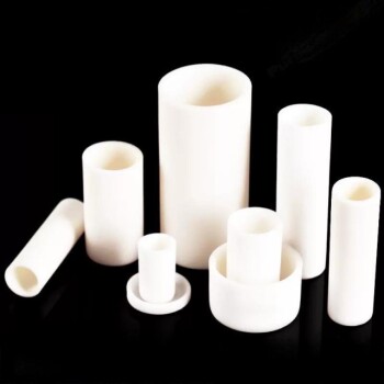
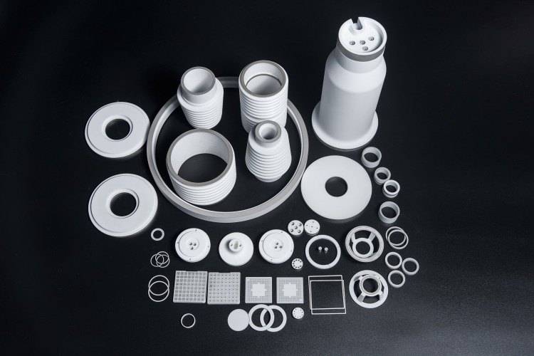
High-purity alumina ceramics, commonly known as aluminum oxide (Al2O3), are integral components in semiconductor manufacturing equipment. These ceramics are renowned for their exceptional mechanical and electrical properties, making them ideal for a variety of critical applications. Specifically, they are utilized in the fabrication of cavity parts, insulation flanges, polishing plates, wafer chucks, and handling arms.
Alumina's high hardness and wear resistance ensure that these components can withstand the rigorous demands of semiconductor production. Additionally, its low erosion levels and high temperature resistance contribute to its durability in environments where thermal stability is paramount. The ceramic's corrosion resistance and bio-inertness further enhance its suitability for use in sensitive semiconductor processes.
Moreover, alumina's high temperature stability and thermal conductivity are particularly advantageous in high-temperature applications, such as thermocouple protection in high-temperature measurements. Precision Ceramics offers a comprehensive range of advanced ceramic tubes and insulators tailored for these specific needs, ensuring optimal performance and reliability in semiconductor manufacturing.
Silicon Carbide (SiC)
Silicon carbide (SiC), also known as carborundum, is a ceramic material renowned for its exceptional heat resistance and mechanical strength, even at temperatures as high as 1400°C. This material is composed of tetrahedra of carbon and silicon atoms, forming a crystal lattice with strong bonds that contribute to its extreme hardness and durability. Unlike many other materials, silicon carbide is not susceptible to attack by acids, alkalis, or molten salts up to 800°C. In air, it forms a protective silicon oxide coating at 1200°C, allowing it to maintain its integrity up to 1600°C.
The unique properties of silicon carbide make it indispensable in various semiconductor manufacturing applications. Its high thermal conductivity, combined with low thermal expansion and high strength, provides exceptional thermal shock resistance, a critical feature for components exposed to rapid temperature changes. Ceramic parts made from silicon carbide, free from grain boundary impurities, retain their strength even at very high temperatures, making them ideal for wafer tray supports and paddles in semiconductor furnaces.
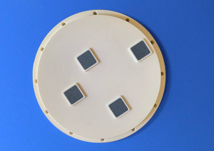
In semiconductor equipment, silicon carbide is utilized in a wide array of components, including XY platforms, pedestals, focusing rings, polishing plates, wafer chucks, vacuum suction cups, handling arms, furnace tubes, wafer boats, and cantilever paddles. These applications leverage silicon carbide's chemical purity, resistance to chemical attack at high temperatures, and strength retention under extreme conditions. Additionally, its electrical conductivity makes it suitable for use in resistance heating elements for electric furnaces and as key components in thermistors and varistors.
The versatility and robustness of silicon carbide ceramics ensure their continued prominence in the semiconductor industry, where precision and reliability are paramount.
Aluminum Nitride (AIN)
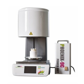
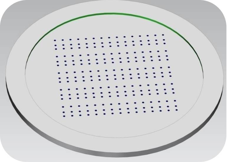
High-purity aluminum nitride (AIN) ceramics are pivotal in semiconductor applications, particularly as wafer heating heaters and electrostatic chucks. This is primarily due to their exceptional thermal conductivity, which surpasses that of many other materials used in semiconductor equipment. The thermal conductivity of AIN is approximately 170-230 W/m·K, making it one of the best thermal conductors among non-metallic materials. This property ensures efficient heat distribution and rapid temperature control, which are critical for maintaining consistent processing conditions during wafer fabrication.
In addition to its thermal conductivity, AIN exhibits remarkable plasma resistance. This characteristic is vital in environments where plasma etching and deposition processes are employed. The material's ability to withstand plasma exposure without degradation or contamination helps maintain the integrity and purity of the semiconductor devices being manufactured. This dual advantage of high thermal conductivity and plasma resistance positions AIN as a superior choice for applications requiring precise thermal management and environmental stability.
The use of AIN in wafer heating heaters and electrostatic chucks is further bolstered by its mechanical stability and low thermal expansion coefficient. These attributes ensure that the material maintains its dimensional integrity under thermal stress, reducing the risk of warping or cracking that could compromise the precision of semiconductor manufacturing processes. As a result, AIN ceramics are not only functional but also reliable, contributing to the overall efficiency and quality of semiconductor production.
Silicon Nitride (Si3N4)
Silicon nitride (Si3N4) stands out as a premier material in the realm of advanced ceramics, boasting an unparalleled combination of mechanical, thermal, and electrical properties. Its exceptional hardness and remarkable thermal shock resistance make it an ideal candidate for applications where materials must endure extreme conditions without compromising performance. Silicon nitride not only surpasses the high-temperature capabilities of most metals but also exhibits superior creep and oxidation resistance, ensuring long-term reliability in high-stress environments.
In semiconductor equipment, silicon nitride is particularly valued for its high fracture toughness, which allows it to withstand the rigors of precision manufacturing processes. Its wear resistance ensures that components maintain their integrity and precision over extended periods, reducing the need for frequent replacements and maintenance. Additionally, silicon nitride's corrosion resistance makes it suitable for use in environments where exposure to harsh chemicals is inevitable, further extending its operational lifespan.
| Property | Silicon Nitride (Si3N4) |
|---|---|
| Hardness | Extremely Hard |
| Thermal Shock Resistance | Exceptional |
| Wear Resistance | High |
| Corrosion Resistance | Superior |
| High-Temperature Capability | Surpasses Most Metals |
Silicon nitride ceramics are widely employed in semiconductor equipment platforms, bearings, and various other critical components. These applications leverage the material's self-lubricating properties, which are particularly beneficial in high-temperature, high-load scenarios. In industries such as aerospace, petroleum, and chemical engineering, silicon nitride's ability to withstand mechanical wear, corrosion, and extreme temperatures makes it a superior choice over traditional metal parts.
In summary, silicon nitride's unique properties position it as a cornerstone material in industries requiring high-performance ceramics. Its ability to meet the stringent demands of semiconductor equipment, along with its versatility in other high-stress applications, underscores its importance in modern engineering.
Overview of Precision Ceramics
Properties and Classification of Precision Ceramics
Precision ceramics are distinguished by their unique properties and are categorized into two primary types: structural ceramics and functional ceramics. Structural ceramics are renowned for their robust mechanical properties, which include high hardness, exceptional abrasion resistance, and superior compressive strength. These materials are designed to withstand extreme conditions, such as high temperatures and thermal shocks, making them indispensable in environments where durability and reliability are paramount.
On the other hand, functional ceramics are characterized by their electrical and magnetic properties. These ceramics are engineered to perform specific functions, such as high dielectric strength and resistance to thermal shocks, which are critical in applications requiring precise control and operation. Unlike ordinary ceramics, which may lack these specialized attributes, precision ceramics are tailored to meet the exacting demands of advanced industries.
The classification of precision ceramics can be further refined based on their chemical composition. The primary groups include:
- Silicate Ceramics: Composed mainly of silicon and oxygen, with other elements such as aluminum and magnesium. These ceramics are known for their thermal stability and electrical insulation properties.
- Non-Oxide Ceramics: Made from materials that do not contain oxygen in their primary structure, such as silicon carbide and boron nitride. These ceramics often exhibit high thermal conductivity and mechanical strength.
- Oxide Ceramics: Comprised of oxides of various metals, including aluminum oxide (alumina) and zirconium oxide. These materials are prized for their excellent dielectric properties and high-temperature stability.
| Ceramic Type | Primary Composition | Key Properties |
|---|---|---|
| Silicate Ceramics | SiO₂, Al₂O₃, MgO | Thermal stability, electrical insulation |
| Non-Oxide Ceramics | SiC, BN | High thermal conductivity, mechanical strength |
| Oxide Ceramics | Al₂O₃, ZrO₂ | Excellent dielectric properties, high-temperature stability |
This detailed classification underscores the diverse applications and capabilities of precision ceramics, ensuring they are perfectly suited for the intricate and demanding requirements of semiconductor equipment.
Manufacturing Process of Precision Ceramics
The manufacturing process of precision ceramics is a complex and multi-stage endeavor, meticulously designed to ensure the production of high-quality components for semiconductor applications. This process begins with the mixing of raw materials, where a precise blend of ceramic powders and additives is created to achieve the desired properties. Following this, the mixture undergoes granulation, a step that enhances the flowability and compactibility of the powder, making it easier to handle during subsequent operations.
Next, the granulated powder is subjected to billet molding, where it is formed into the rough shape of the final product. This is typically achieved through techniques such as pressing or injection molding, which compact the powder into a green body. The green body is then subjected to billet processing, which involves trimming and refining the shape to meet the exact specifications required for semiconductor equipment.
The most critical stage in the process is sintering, where the green body is heated to a high temperature in a controlled environment. During sintering, the volatile components, such as moisture and organic additives, are removed, and the ceramic particles bond together to form a dense, strong structure. The shrinkage that occurs during this process is carefully managed through the use of a shrinkage coefficient, which allows for precise calculation of the final dimensions of the part.
Once sintered, the ceramic part undergoes finishing, a series of machining operations that refine the surface and dimensions to meet the stringent tolerances required for semiconductor applications. These operations, which include grinding, milling, drilling, and polishing, are often performed using diamond tooling or ultrasound due to the hardness and brittleness of the material. The final step in the process is quality testing, where the part is inspected for defects and dimensional accuracy, followed by surface treatment to enhance its performance and durability in the harsh environments of semiconductor manufacturing.
Related Products
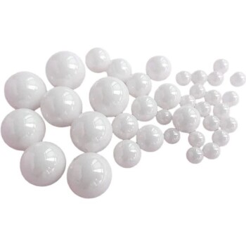
- Precision Machined Zirconia Ceramic Ball for Engineering Advanced Fine Ceramics
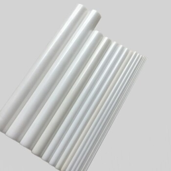
- Precision Machined Yttrium Stabilized Zirconia Ceramic Rod for Engineering Advanced Fine Ceramics
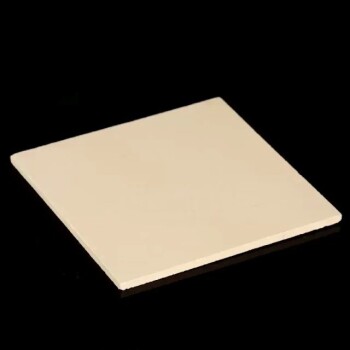
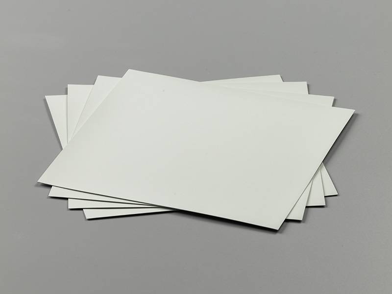
- Precision Machined Silicon Nitride (SiN) Ceramic Sheet for Engineering Advanced Fine Ceramics
- Precision Machined Yttria Stabilized Zirconia Ceramic Plate for Engineering Advanced Fine Ceramics
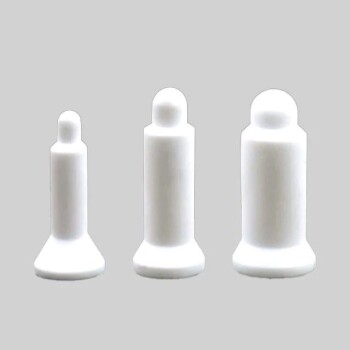
- Engineering Advanced Fine Alumina (Al₂O₃) Ceramic Positioning Pin Straight Bevel for Precision Applications
Related Articles
- Zirconia Ceramic Rod Production Processes: Isostatic Pressing vs. Dry Pressing
- Research on Zirconia Ceramics in Dental Restoration
- Engineering Ceramic Materials: Applications in Aerospace, Electronic Information, New Energy, and Environmental Protection
- Precision Ceramic Materials for Energy Conversion Applications
- Advancements in Engineering Ceramic Materials