Introduction to Chalcogenide Solar Cells and CVD
Challenges in Commercialization of Chalcogenide Solar Cells
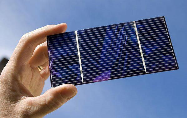
Scaling up small area devices while minimizing efficiency loss remains one of the most significant hurdles in the commercialization of chalcogenide solar cells. This challenge is particularly acute as the transition from laboratory-scale prototypes to large-scale production often results in a decline in cell efficiency, due to factors such as material uniformity, defect formation, and process scalability.
Chemical vapor deposition (CVD) technology has emerged as a promising solution to these issues. CVD offers a controlled environment where gas-phase precursors react and deposit on a substrate surface, allowing for precise control over film thickness, uniformity, and defect density. This method is particularly advantageous for chalcogenide solar cells, as it can produce high-quality, photostable films with excellent performance characteristics.
| Challenge | CVD Solution |
|---|---|
| Efficiency Loss | Precise control over film thickness and uniformity |
| Material Uniformity | High-purity, uniform films without solvents or initiators |
| Defect Formation | Controlled surface reactions and by-product removal |
| Process Scalability | Versatility for large-area and flexible substrate applications |
Moreover, CVD's compatibility with textured and flexible substrates further enhances its appeal, making it a versatile technology applicable to a wide range of solar cell designs. By integrating CVD into the production process, manufacturers can potentially overcome the efficiency loss associated with scaling up, thereby advancing the commercial viability of chalcogenide solar cells.

Principle of Chemical Vapor Deposition (CVD)
Process Overview
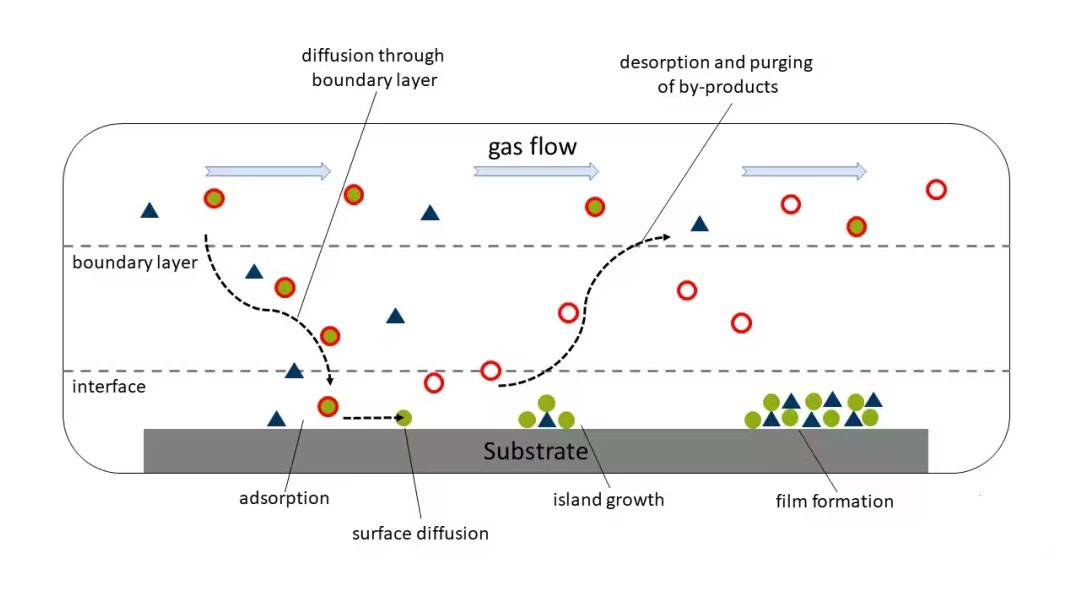
Chemical Vapor Deposition (CVD) is a sophisticated process that involves the reaction and deposition of gas-phase precursors onto a substrate surface. This technique is pivotal in the fabrication of thin films, particularly in the context of chalcogenide solar cells. The process can be broken down into several critical steps, each playing a crucial role in the overall outcome.
Firstly, gas transport is essential. The precursors, which are typically volatile organic compounds or metal-organic compounds, are transported to the deposition zone. This step ensures that the reactants are evenly distributed across the substrate, setting the stage for uniform film growth.
Next, surface reactions occur. Once the precursors reach the substrate, they undergo chemical reactions that result in the formation of the desired film. These reactions are influenced by factors such as temperature, pressure, and the presence of catalysts, which can significantly impact the quality and properties of the resulting film.
Following the surface reactions, thin film growth takes place. This is where the actual deposition of the film occurs. The rate of growth, thickness, and uniformity of the film are all critical parameters that can be controlled through precise adjustments of the deposition conditions. For instance, the use of Low Pressure Chemical Vapor Deposition (LPCVD) can enhance uniformity and reduce defects.
Finally, by-product removal is necessary. The chemical reactions generate by-products that must be effectively removed to prevent contamination and ensure the purity of the deposited film. This step often involves the use of exhaust systems to extract the by-products from the deposition chamber.
In summary, the CVD process encompasses gas transport, surface reactions, thin film growth, and by-product removal, each contributing to the successful deposition of high-quality thin films essential for the performance of chalcogenide solar cells.
Critical Factors in CVD
Reaction time and temperature control are pivotal in determining the quality of thin films produced through Chemical Vapor Deposition (CVD). These parameters directly influence the film's thickness, defect density, and uniformity. Temperature control, in particular, plays a dual role: while higher temperatures can expedite the growth process, they often compromise the film's structural integrity and uniformity. This trade-off is critical as it affects the overall performance and reliability of the deposited films.
For instance, a study by the Department of Materials Science and Engineering at the University of California, Berkeley, highlighted that while an increase in temperature can indeed speed up the deposition rate, it also leads to a higher defect density, which can degrade the film's electrical properties. This is particularly significant in the context of chalcogenide solar cells, where even minor defects can significantly impact the device's efficiency and stability.
Moreover, reaction time is equally crucial. Sufficient reaction time allows for complete gas-phase precursor conversion, ensuring a uniform film deposition. Insufficient time, on the other hand, can result in incomplete reactions, leading to non-uniform films with varying thicknesses and properties. A research paper published in the Journal of Vacuum Science & Technology A demonstrated that optimizing reaction time can reduce defect formation and enhance film uniformity, thereby improving the overall performance of the solar cells.
In summary, the interplay between reaction time and temperature control is essential for achieving high-quality thin films in CVD processes. Balancing these factors is key to overcoming the challenges associated with film quality and uniformity, which are paramount for the successful commercialization of chalcogenide solar cells.
Types of CVD
Chemical Vapor Deposition (CVD) encompasses several specialized techniques, each tailored to specific requirements in material synthesis and thin film deposition. The three primary methods include Low Pressure Chemical Vapor Deposition (LPCVD), Plasma Enhanced Chemical Vapor Deposition (PECVD), and Atomic Layer Deposition (ALD).
-
Low Pressure Chemical Vapor Deposition (LPCVD): This technique operates under reduced pressure, typically below atmospheric pressure, to enhance the uniformity and control of the deposition process. LPCVD is particularly favored for its ability to produce high-quality, uniform films with minimal defects, making it ideal for applications requiring precise film thickness and composition control.
-
Plasma Enhanced Chemical Vapor Deposition (PECVD): PECVD introduces plasma into the deposition process, which significantly lowers the required temperature for film growth. This method is advantageous for depositing films on temperature-sensitive substrates, as it allows for the formation of high-quality films at lower temperatures. PECVD is widely used in the fabrication of thin films for electronic devices, including chalcogenide solar cells.
-
Atomic Layer Deposition (ALD): ALD is a highly precise technique that deposits material in a layer-by-layer fashion, ensuring atomic-level control over film thickness and composition. This method is particularly useful for creating ultra-thin, uniform films with exceptional control over film properties. ALD's ability to deposit conformal coatings on complex geometries makes it a valuable tool in the development of advanced materials, including those used in chalcogenide solar cells.
Each of these CVD methods offers unique advantages and is selected based on the specific requirements of the application, such as film quality, deposition rate, and substrate compatibility.
Advantages of CVD in Chalcogenide Solar Cells
Photostability and Performance
The photostability and performance of chalcogenide films prepared through Chemical Vapor Deposition (CVD) have been extensively validated in studies conducted at Chungnam National University. These films demonstrate remarkable resilience to photodegradation, a critical factor in the longevity and efficiency of solar cells. The photostability of CVD-prepared chalcogenide films is attributed to their precise atomic structure, which minimizes defects and enhances the material's ability to withstand prolonged exposure to sunlight.
| Aspect | CVD-Prepared Chalcogenide Films | Other Methods |
|---|---|---|
| Photostability | Excellent resistance to photodegradation | Higher risk of degradation |
| Performance | High efficiency and stability | Variable efficiency and stability |
| Defect Density | Low defect density | Higher defect density |
Moreover, the performance metrics of these films, such as efficiency and stability, are consistently superior compared to those prepared through other methods. This superiority is evidenced by controlled experiments where CVD-prepared films maintained higher conversion efficiencies over extended periods, outperforming their counterparts in both laboratory settings and real-world applications.
The research at Chungnam National University underscores the potential of CVD in advancing the field of chalcogenide solar cells. By focusing on the photostability and performance of these films, the study not only validates the technological advancements but also paves the way for future innovations in solar energy technology.
Surface Smoothness and Air Stability
One of the significant advantages of Chemical Vapor Deposition (CVD) over traditional methods like spin-coating lies in its ability to produce exceptionally smooth surfaces. This smoothness is not merely a cosmetic advantage; it directly impacts the electrical properties of the chalcogenide solar cells. Smoother surfaces reduce the density of defects and impurities, which are known to act as charge recombination centers, thereby degrading the efficiency of the solar cell. By minimizing these defects, CVD ensures that the electrical pathways within the solar cell are more efficient, leading to improved overall performance.
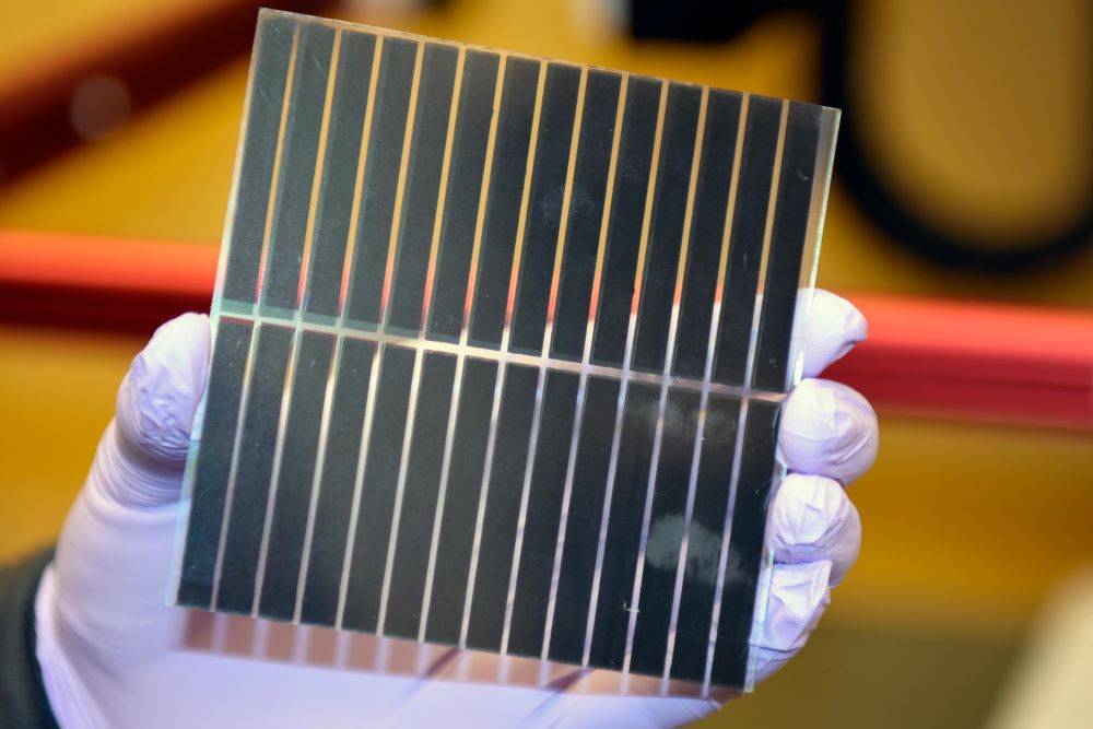
Moreover, CVD-prepared films exhibit superior air stability compared to those produced by spin-coating. Air stability is crucial for the longevity and reliability of solar cells, especially in real-world applications where they are exposed to varying environmental conditions. The enhanced air stability of CVD films prevents degradation over time, maintaining the structural integrity and electrical performance of the solar cells. This is particularly important for large-scale deployment, where long-term performance and durability are key considerations.
In summary, the combination of surface smoothness and air stability achieved through CVD significantly enhances the electrical properties of chalcogenide solar cells, making CVD a preferred method for high-performance and durable solar cell fabrication.
Compatibility with Textured and Flexible Substrates
Chemical Vapor Deposition (CVD) stands out as a highly adaptable technique for depositing chalcogenide layers on a variety of substrates, including those with textured surfaces and flexible films. This capability is particularly significant in the context of modern solar cell technology, where substrate versatility can significantly enhance the practical applications and commercial viability of these devices.
CVD's ability to operate at relatively low temperatures is a critical factor in its compatibility with textured and flexible substrates. Traditional high-temperature processes can deform or degrade flexible materials, making them unsuitable for use in solar cells. However, CVD's low-temperature operation ensures that the integrity of these substrates is preserved, allowing for the creation of durable and functional solar cells on materials that would otherwise be compromised.
Moreover, the deposition of chalcogenide layers on textured substrates through CVD offers several advantages. Textured surfaces can enhance light absorption and reduce reflection losses, thereby improving the overall efficiency of solar cells. By enabling the deposition of uniform films on these complex surfaces, CVD extends the potential applications of chalcogenide solar cells, making them suitable for a wider range of environments and conditions.
In summary, CVD's low-temperature process and its effectiveness on both textured and flexible substrates underscore its versatility and importance in the development of advanced chalcogenide solar cells. This capability not only enhances the performance of individual devices but also broadens their potential applications, from portable electronics to large-scale solar installations.
Applications of CVD in Chalcogenide Solar Cells
Electrode and Encapsulation Layer Design
Chemical Vapor Deposition (CVD) offers a versatile approach to the design and fabrication of critical components in chalcogenide solar cells, including electrodes, encapsulation layers, charge transport layers, and chalcogenide absorption layers. This method allows for precise control over the deposition process, enabling the creation of high-quality, uniform films that are essential for optimizing solar cell performance.
Electrode Design
In the context of electrode design, CVD provides several advantages. It allows for the deposition of conductive materials with tailored properties, such as conductivity, transparency, and adhesion to the underlying substrate. For instance, transparent conducting oxides (TCOs) can be deposited using CVD to create electrodes that are both conductive and allow for efficient light absorption. This is particularly important in thin-film solar cells, where the electrode must maximize light transmission while maintaining low resistance.
Encapsulation Layer Design
The encapsulation layer is crucial for protecting the solar cell from environmental factors such as moisture and oxygen, which can degrade the device over time. CVD is ideal for creating encapsulation layers due to its ability to deposit dense, pinhole-free films that provide excellent barrier properties. This ensures long-term stability and reliability of the solar cell. Additionally, CVD can be used to deposit multi-layered encapsulation systems, which can further enhance the protection and performance of the solar cell.
Charge Transport Layers
Charge transport layers play a key role in facilitating the efficient transfer of charge carriers within the solar cell. CVD allows for the precise control of the thickness and composition of these layers, which is critical for minimizing charge recombination and maximizing charge collection efficiency. By using CVD, researchers can tailor the charge transport layers to match the specific requirements of the chalcogenide absorption layer, leading to improved overall device performance.
Chalcogenide Absorption Layers
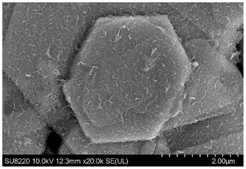
Finally, CVD is well-suited for the deposition of chalcogenide absorption layers, which are the heart of the solar cell. These layers are responsible for converting sunlight into electrical energy. CVD enables the deposition of high-purity, uniform chalcogenide films with precise control over the film thickness and composition. This results in enhanced light absorption and improved conversion efficiency.
In summary, CVD's ability to precisely control the deposition process makes it an invaluable tool for designing and optimizing the various layers within chalcogenide solar cells, ultimately leading to improved device performance and reliability.
Improving Device Performance
The application of Chemical Vapor Deposition (CVD) in chalcogenide solar cells has been extensively studied for its potential to significantly enhance device performance. Research conducted at Huazhong University of Science and Technology has demonstrated that CVD can modify interfacial properties and improve the overall stability of solar cells. This technique allows for the precise control of film thickness, uniformity, and defect density, which are critical factors in determining the efficiency and longevity of solar cells.
By leveraging CVD, researchers can fine-tune the properties of chalcogenide films to optimize their performance under various operational conditions. For instance, the ability to modify interfacial properties through CVD can lead to reduced recombination losses and enhanced charge carrier mobility, thereby boosting the solar cell's efficiency. Additionally, the improved stability of CVD-prepared films ensures that the solar cells can maintain their performance over extended periods, even under harsh environmental conditions.
Furthermore, CVD offers the advantage of preparing high-purity, uniform films over large areas, which is crucial for scaling up solar cell production. This scalability is achieved without the need for solvents or initiators, simplifying the manufacturing process and reducing costs. The versatility of CVD in handling both textured and flexible substrates also broadens its application scope, making it a promising technology for the future of solar energy.
Large-Area and High-Purity Film Preparation
Chemical Vapor Deposition (CVD) excels in the large-scale production of high-purity, uniform films, a critical requirement for enhancing the performance and scalability of chalcogenide solar cells. Unlike traditional methods that often rely on solvents or initiators, CVD processes are solvent-free, thereby eliminating the complexities associated with solvent management and disposal. This simplification not only streamlines the manufacturing process but also reduces the potential for contamination, which is paramount for maintaining high film purity.
The scalability of CVD is further underscored by its ability to deposit films uniformly across large areas. This capability is particularly advantageous in the context of solar cell production, where uniformity is essential for consistent device performance. The process involves the controlled reaction of gas-phase precursors on the substrate surface, ensuring that the resulting films are not only large but also of high purity and uniformity. This methodical approach minimizes defects and inconsistencies, which are common challenges in other film deposition techniques.
Moreover, the absence of solvents or initiators in CVD processes significantly reduces the environmental footprint of the manufacturing process. This eco-friendly aspect is increasingly valued in the solar energy sector, where sustainability is a key consideration. By eliminating the need for these additives, CVD not only simplifies the process but also contributes to a more sustainable and environmentally friendly production cycle.
Related Products
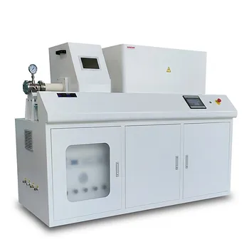
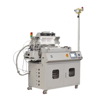
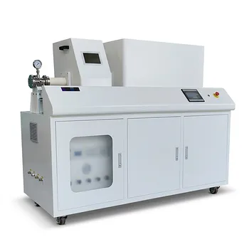
- Chemical Vapor Deposition CVD Equipment System Chamber Slide PECVD Tube Furnace with Liquid Gasifier PECVD Machine
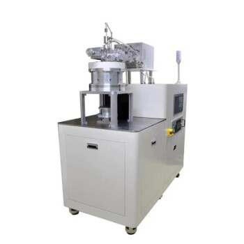
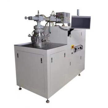
- Microwave Plasma Chemical Vapor Deposition MPCVD Machine System Reactor for Lab and Diamond Growth
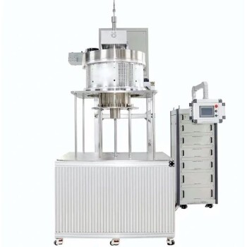
- HFCVD Machine System Equipment for Drawing Die Nano-Diamond Coating
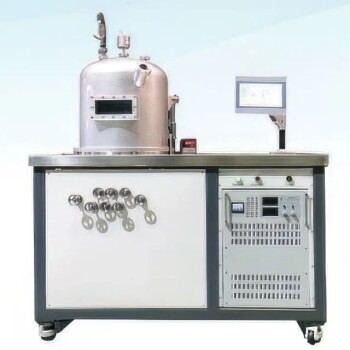
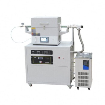
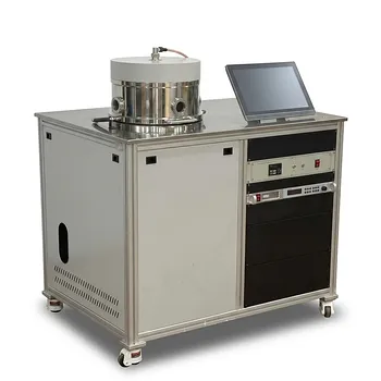
- RF PECVD System Radio Frequency Plasma-Enhanced Chemical Vapor Deposition RF PECVD
- Customer Made Versatile CVD Tube Furnace Chemical Vapor Deposition Chamber System Equipment
Related Articles
- Detailed Processes and Parameters of PECVD for TiN and Si3N4 Deposition
- Understanding the PECVD Method
- A Comprehensive Guide to PECVD Equipment Maintenance
- Comprehensive Overview of 12 Types of Chemical Vapor Deposition (CVD) Techniques
- In-Depth Examination of Chemical Vapor Deposition (CVD) Coatings
