Introduction to Graphene and Its Preparation
Historical Background and Discovery of Graphene
The study of carbon nanomaterials has been a focal point in materials research since the discovery of fullerenes in 1985 and carbon nanotubes in 1991. These materials, characterized by their unique structural and electronic properties, opened new avenues for scientific exploration. Among these, graphene stands out as a particularly intriguing material. Initially, graphene was considered thermodynamically unstable due to its two-dimensional structure, which defied classical physics principles. However, in 2004, scientists at the University of Manchester successfully isolated graphene, a groundbreaking achievement that redefined the boundaries of material science.
The isolation of graphene was achieved through a simple yet ingenious method involving the mechanical exfoliation of graphite using adhesive tape. This method, developed by Andre Geim and Konstantin Novoselov, not only demonstrated the feasibility of producing single-layer graphene but also ignited a surge of interest in its potential applications. The discovery of graphene was quickly followed by numerous studies exploring its remarkable properties, including high electrical conductivity, exceptional mechanical strength, and thermal conductivity. These properties, combined with its atomic-scale thickness, positioned graphene as a material with unparalleled potential across various fields, from electronics to composites.
The successful isolation of graphene also challenged long-held beliefs about the limitations of two-dimensional materials. This breakthrough not only validated the existence of stable two-dimensional carbon structures but also spurred further research into other two-dimensional materials, broadening the scope of nanomaterials research. The discovery of graphene, therefore, not only advanced the understanding of carbon-based materials but also laid the foundation for future innovations in material science.

Importance of Material Preparation
The meticulous preparation of materials is indispensable for delving into their intrinsic properties and uncovering their myriad applications. Over the years, the scientific community has engineered a plethora of methods for graphene preparation, each contributing to significant enhancements in both yield and quality. These advancements have not only facilitated a deeper understanding of graphene's unique characteristics but have also spurred a wave of research aimed at harnessing its potential in various fields.
One of the most notable methods is the Chemical Vapor Deposition (CVD) technique, which has emerged as a cornerstone in the synthesis of high-quality, large-area graphene. This method, which involves the decomposition of carbon-containing compounds at elevated temperatures on substrate surfaces, has been widely adopted due to its simplicity and efficacy. The resulting graphene, produced through controlled environments and precise conditions, boasts exceptional properties that are crucial for both fundamental research and practical applications.
Moreover, the development of graphene preparation techniques has been a collaborative effort, drawing insights from diverse scientific disciplines. For instance, the tape stripping method, pioneered by Geim's group, and the chemical stripping method, which leverages functional groups to separate graphene oxide layers, have each offered unique advantages and contributed to the broader knowledge base. These methods, alongside others like the Silicon Carbide (SiC) epitaxial growth method, highlight the multifaceted approach to graphene synthesis.
In essence, the evolution of graphene preparation techniques underscores the importance of material preparation in driving scientific inquiry and technological innovation. As research continues to refine these methods, the potential applications of graphene are poised to expand, promising breakthroughs in energy, electronics, and beyond.
Main Preparation Methods of Graphene
Tape Stripping Method
The tape stripping method, pioneered by Geim's group in 2004, represents a groundbreaking technique for the isolation of graphene. This method leverages the adhesive properties of tapes to systematically strip layers of highly oriented pyrolytic graphite (HOPG) and flake graphite. By repeatedly applying and peeling off adhesive tapes, researchers can meticulously remove layers until monolayers and a few layers of graphene are obtained.
This technique is particularly noteworthy for its simplicity and effectiveness in producing high-quality graphene. The process involves adhering the tape to the graphite surface, pressing firmly to ensure good contact, and then quickly peeling it off. This action dislodges and transfers the topmost layers of graphite onto the tape. Repeating this process multiple times gradually reduces the thickness of the remaining graphite until single or few-layer graphene is achieved.
The resulting graphene layers are then transferred onto various substrates, with silicon wafers being a common choice due to their compatibility with subsequent characterization and application processes. This method has been instrumental in early studies of graphene's properties, providing a reliable means to obtain samples for further research.
| Advantages | Limitations |
|---|---|
| Simple and cost-effective | Labor-intensive and time-consuming |
| Produces high-quality monolayers | Limited scalability for large-area production |
| Suitable for fundamental research | Requires careful handling to avoid contamination |
Despite its limitations, the tape stripping method remains a cornerstone in the history of graphene research, demonstrating the ingenuity and resourcefulness of early pioneers in the field.
Chemical Stripping Method
The chemical stripping method is a sophisticated technique used to prepare graphene by introducing functional groups to graphite layers. This process significantly increases the spacing between the layers, facilitating the separation of graphene oxide layers through methods such as ultrasound or rapid expansion.
Ultrasound, in particular, is a powerful tool in this process. It creates mechanical vibrations that can effectively disrupt the interlayer bonds of graphite, aiding in the exfoliation of graphene oxide. Similarly, rapid expansion techniques can be employed to achieve a similar effect, often utilizing sudden changes in pressure or temperature to separate the layers.
Once the graphene oxide is successfully separated, the next step involves its reduction. This reduction process is crucial as it transforms the graphene oxide into pure graphene. Various reduction methods can be applied, including chemical reduction using agents like hydrazine or thermal reduction through high-temperature treatments. Each method has its own set of advantages and challenges, influencing the final quality and properties of the graphene produced.
This method is particularly notable for its ability to produce large quantities of graphene with relatively high efficiency. However, it also requires careful control of the chemical and physical parameters to ensure the quality of the final product. The resulting graphene, after reduction, exhibits enhanced electrical, thermal, and mechanical properties, making it highly suitable for a wide range of applications in materials science and technology.
Silicon Carbide (SiC) Epitaxial Growth Method
The epitaxial growth of graphene on silicon carbide (SiC) substrates involves a sophisticated process under high-temperature and ultra-high vacuum conditions. During this process, silicon atoms are volatilized, leaving behind carbon atoms that coalesce to form a graphene layer on the SiC surface. This method is particularly advantageous for producing large-area monolayer graphene with exceptional quality, making it a preferred technique for various electronic applications.
In addition to the high-temperature and vacuum conditions, the epitaxial growth method can be further enhanced by incorporating chemical vapor deposition (CVD) techniques. This allows for the growth of 3C- and 6H- silicon carbide (SiC) on silicon wafer substrates, which can be tailored to introduce n-type and p-type dopants into the monocrystalline SiC films. While there are other methods to create silicon carbide crystals, CVD has proven to be a cost-effective approach for developing relatively thick, impurity-free SiC crystals, which are essential for high-performance electronics manufacturing.
The combination of these techniques not only ensures the formation of high-quality graphene but also enables the integration of advanced functionalities, such as doping, which can significantly enhance the electronic properties of the resulting graphene layers. This makes the SiC epitaxial growth method a versatile and powerful tool in the arsenal of graphene production methods.
Chemical Vapor Deposition (CVD) Method
Chemical Vapor Deposition (CVD) is a sophisticated vacuum deposition technique widely employed in the semiconductor industry for producing high-quality, high-performance solid materials, particularly thin films. This method involves exposing a substrate, typically a wafer, to one or more volatile precursors. These precursors undergo chemical reactions or decomposition processes on the substrate's surface, resulting in the deposition of the desired material. Common by-products of these reactions are typically removed through gas flow within the reaction chamber, ensuring a clean deposition environment.
In the context of graphene production, CVD leverages methane and other carbon-containing compounds as the primary carbon source. The process involves high-temperature decomposition of these compounds on the substrate's surface, facilitating the growth of graphene layers. This technique is particularly favored for its simplicity, which translates into ease of operation and scalability. Moreover, CVD excels in producing high-quality graphene, characterized by its structural integrity and electronic properties. The method's capability for large-area growth further enhances its appeal, making it a cornerstone in the fabrication of graphene-based devices and materials.
CVD is practiced in various formats, each differing in how chemical reactions are initiated. Key types include:
- Hot-wall thermal CVD: Operates in a batch mode, suitable for controlled, large-scale production environments.
- Plasma-assisted CVD: Utilizes plasma to enhance reaction rates and improve the quality of the deposited material.
These variations underscore the versatility and adaptability of CVD, making it a versatile tool in the arsenal of graphene preparation methods.
Preparation of Graphene by CVD Method
CVD Growth Mechanisms
The Chemical Vapor Deposition (CVD) process for graphene synthesis involves two primary mechanisms: carburization and surface growth. These mechanisms differ significantly depending on the type of metal substrate used, such as nickel or copper.
For metal substrates like nickel, the carburization process is dominant. In this process, carbon atoms are introduced into the vacuum environment and penetrate the nickel substrate. As the temperature is increased, the carbon atoms diffuse into the nickel lattice, leading to the formation of nickel carbide. Upon cooling, the supersaturated carbon atoms precipitate out of the nickel lattice, forming graphene layers on the surface. This mechanism is characterized by the formation of large, continuous graphene sheets.
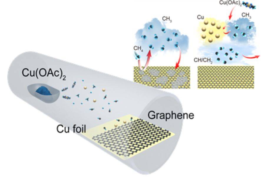
In contrast, copper substrates primarily facilitate a surface growth mechanism. Here, carbon atoms adsorb onto the copper surface at elevated temperatures. These carbon atoms then nucleate and grow into graphene islands. Unlike the carburization process, the surface growth mechanism results in the formation of smaller, isolated graphene domains. The small footprint and excellent process control of Microwave Plasma CVD (MPCVD) enhance the efficiency of this surface growth process, making it a popular choice for graphene synthesis.
| Growth Mechanism | Metal Substrate | Process | Outcome |
|---|---|---|---|
| Carburization | Nickel | Carbon atoms penetrate and diffuse into the substrate, forming nickel carbide, which precipitates into graphene upon cooling. | Large, continuous graphene sheets. |
| Surface Growth | Copper | Carbon atoms adsorb onto the surface, nucleate, and grow into graphene islands. | Small, isolated graphene domains. |
Carbon Source Selection
Hydrocarbon gases such as methane, ethylene, and acetylene are commonly employed as carbon sources in the Chemical Vapor Deposition (CVD) process for graphene synthesis. The selection of these gases is not arbitrary; it directly influences the growth temperature and the structural integrity of the resulting graphene layers. For instance, methane is often preferred for its stability and ease of decomposition at moderate temperatures, while ethylene can facilitate faster growth rates due to its higher carbon content.
| Carbon Source | Typical Growth Temperature | Advantages | Disadvantages |
|---|---|---|---|
| Methane | 900-1100°C | Stable, easy to decompose | Slower growth rates |
| Ethylene | 700-900°C | Faster growth rates | Higher risk of defects |
| Acetylene | 600-800°C | Very fast growth | High defect formation |
The choice of carbon source also impacts the quality and uniformity of the graphene produced. For example, using acetylene can lead to the rapid formation of graphene but may also introduce more defects due to the high reactivity of the gas. Conversely, methane, though slower, tends to yield higher quality graphene with fewer defects.
In addition to conventional methods, plasma-assisted CVD has emerged as a promising technique to reduce the growth temperature while maintaining high-quality graphene production. This method leverages the high energy of plasma to enhance the decomposition of hydrocarbons, thereby lowering the thermal budget required for graphene growth. This is particularly beneficial for substrates that cannot withstand high temperatures, expanding the range of materials that can be used for graphene synthesis.
By carefully selecting the carbon source and employing advanced techniques like plasma-assisted CVD, researchers can optimize the growth conditions to achieve high-quality, large-area graphene, which is essential for its practical applications in electronics, energy, and composites.
Growth Substrate Considerations
When employing Chemical Vapor Deposition (CVD) for graphene synthesis, the choice of growth substrate is pivotal. Commonly used metal foils include nickel and copper, each offering distinct advantages and challenges.
Key Factors in Substrate Selection
| Factor | Nickel | Copper |
|---|---|---|
| Melting Point | Higher melting point, allowing for higher processing temperatures. | Lower melting point, necessitating more controlled growth conditions. |
| Dissolved Carbon Amount | Higher solubility for carbon, facilitating the formation of graphene layers. | Lower solubility, leading to surface-bound graphene growth. |
| Stability of Metal Carbides | Stable carbides form, aiding in the nucleation and growth of graphene. | Less stable carbides, which can complicate the growth process. |
Nickel's higher melting point enables it to withstand higher processing temperatures, which is crucial for the decomposition of carbon sources. However, its high carbon solubility means that carbon atoms can penetrate deep into the substrate, potentially leading to the formation of multi-layer graphene. In contrast, copper's lower melting point requires more precise temperature control, but its lower carbon solubility promotes the growth of single-layer graphene, which is often preferred for many applications.
The stability of metal carbides also plays a significant role. Stable carbides in nickel substrates can provide a more controlled environment for graphene nucleation and growth, whereas the less stable carbides in copper can introduce variability in the graphene formation process.
In summary, while both nickel and copper substrates have their merits, the selection ultimately hinges on the desired graphene properties and the specific requirements of the application.
Growth Conditions
Growth conditions in Chemical Vapor Deposition (CVD) for graphene synthesis are critical parameters that significantly influence the quality and yield of the resulting graphene. These conditions include gas pressure, carrier gas type, and growth temperature. Each of these factors plays a distinct role in the formation and characteristics of the graphene layers.
Gas Pressure: The pressure within the CVD reactor can affect the diffusion and residence time of carbon atoms on the substrate. Higher pressures can lead to increased carbon atom collisions, potentially enhancing the nucleation and growth of graphene. Conversely, lower pressures can reduce the likelihood of defects, resulting in higher quality graphene.
Carrier Gas Type: The choice of carrier gas, such as hydrogen, argon, or nitrogen, can influence the interaction between the carbon source and the substrate. Hydrogen, for instance, is known to assist in the etching of non-carbon species, leading to cleaner graphene surfaces. Argon, on the other hand, provides a more inert environment, which can be beneficial for precise control over the growth process.
Growth Temperature: The temperature at which the CVD process occurs is a pivotal factor. High temperatures promote the dissociation of carbon-containing gases, facilitating the formation of graphene layers. However, excessively high temperatures can also lead to the formation of defects or even the degradation of the substrate. Therefore, optimizing the growth temperature is essential for achieving both high quality and high yield.
| Growth Condition | Influence on Graphene Quality and Yield |
|---|---|
| Gas Pressure | Affects diffusion and residence time |
| Carrier Gas Type | Influences interaction with carbon source |
| Growth Temperature | Promotes dissociation and layer formation |
Understanding and precisely controlling these growth conditions are key to advancing the CVD method for large-scale, high-quality graphene production.
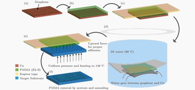
Graphene Transfer Technology
Importance of Graphene Transfer
Graphene transfer technology is indispensable for the characterization, physical property measurement, and application research of graphene. The ability to seamlessly shift graphene from its growth substrate to a target substrate without compromising its structural integrity is pivotal. This process ensures that graphene retains its pristine properties, which are essential for its myriad applications in electronics, optoelectronics, and energy storage.
The transfer process must adhere to stringent criteria: maintaining film continuity without introducing mechanical damage such as cracks, holes, or wrinkles; ensuring the film remains residue-free and undoped; and achieving a stable, reliable, and cost-effective method suitable for industrialization. Various transfer methods have been developed, each with its unique approach to meeting these criteria.
One significant advancement in transfer technology involves the use of polymethyl methacrylate (PMMA) as a sacrificial layer. This method involves coating graphene with PMMA, etching away the underlying metal substrate, and transferring the graphene/PMMA film to the desired substrate. Post-transfer, the PMMA is removed using acetone, leaving a clean graphene film on the target substrate. This method has proven effective in transferring both full wafer graphene from copper foil and nickel film onto substrates like glass, Si/SiO2, and polyethylene terephthalate (PET) films.
The invention of graphene transfer technology has not only facilitated the discovery and characterization of graphene but also opened new avenues for its application. For instance, the transfer process enables the integration of graphene into sensors, enhancing their sensitivity and reliability. This is particularly relevant in applications such as automotive glazing, ballistic covers, and protective gear, where the presence of damage can be detected with high precision, thereby significantly improving user safety.
In summary, graphene transfer technology is a cornerstone in the advancement of graphene research and its practical applications. It ensures that graphene retains its unique properties, enabling its use in a wide range of high-tech applications, from nanoelectronics to advanced materials science.

Etching Substrate Method
The etching substrate method is a pivotal technique in graphene transfer technology, enabling the seamless migration of graphene from its growth substrate to a target substrate. This method employs transfer media such as Polymethyl methacrylate (PMMA) or Polydimethylsiloxane (PDMS) to facilitate the separation process. These materials are chosen for their ability to adhere to graphene while maintaining its structural integrity.
Once the graphene is securely bonded to the transfer medium, it is carefully lifted from the growth substrate. This step requires precision to avoid damaging the delicate graphene layers. The transfer medium then acts as a protective shield, allowing the graphene to be placed onto the desired target substrate without contamination or degradation.
After the graphene is successfully transferred, the transfer medium is removed through a controlled process. This removal is typically achieved through chemical dissolution or thermal decomposition, ensuring that the graphene remains intact on the new substrate. The result is a high-quality graphene layer that is ready for further characterization, physical property measurement, and application research.
This method is particularly advantageous for its ability to handle large-area graphene transfers, which is crucial for industrial applications. However, it also presents challenges such as minimizing defects and ensuring uniform coverage, which are areas of ongoing research. Future advancements in this field may focus on developing more efficient and less damaging transfer media, as well as exploring new substrates that can further enhance the quality and applicability of transferred graphene.
Challenges and Future Directions
Despite significant advancements in graphene production through Chemical Vapor Deposition (CVD), several challenges persist, particularly in the transfer process. The primary concern is the integrity of large-area graphene during transfer, as damage or contamination can significantly degrade its quality and performance.
Future research directions in this field are multifaceted. One promising avenue is the development of more sophisticated transfer methods. For instance, researchers are exploring the use of novel polymers and surface treatments to enhance the adhesion and stability of graphene during the transfer process. Additionally, the introduction of automated systems could minimize human error and improve the consistency of graphene transfers.
Another critical area of focus is the exploration of new substrates. Traditional substrates like copper and nickel have limitations in terms of scalability and quality. Emerging substrates, such as certain transition metal nitrides and oxides, are being investigated for their potential to support high-quality graphene growth without the need for complex transfer processes. These materials offer unique properties that could simplify the production pipeline and reduce contamination risks.
Furthermore, the integration of advanced characterization techniques is essential for monitoring the quality of graphene during and after transfer. Tools like atomic force microscopy (AFM) and Raman spectroscopy can provide real-time feedback, allowing for immediate adjustments to the transfer process to ensure optimal results.
In summary, while the transfer of large-area graphene remains a significant challenge, ongoing research is paving the way for innovative solutions. By improving transfer methods, exploring new substrates, and leveraging advanced characterization techniques, the future of high-quality graphene production looks promising.
Conclusion and Future Prospects
Summary of Graphene's Development
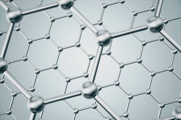
Graphene's unique properties and broad applications have driven rapid advancements in its preparation methods. From the initial isolation by mechanical exfoliation in 2004 by Professors Andre Geim and Kostya Novoselov at the University of Manchester, the field of graphene research has seen exponential growth. Graphene, a two-dimensional, single-atomic layer material consisting of six bonded sp2 carbon atoms in a honeycomb lattice, exhibits remarkable properties such as ultrahigh electron mobility, high Young’s modulus, and exceptional thermal and electrical conductivity.
These extraordinary properties have paved the way for diverse applications, including electronics, composites, membranes, and next-generation renewable energy technologies like solar cells. The significant theoretical specific surface area of graphene, coupled with its flexibility and strength, makes it a versatile material with immense potential across various industries.
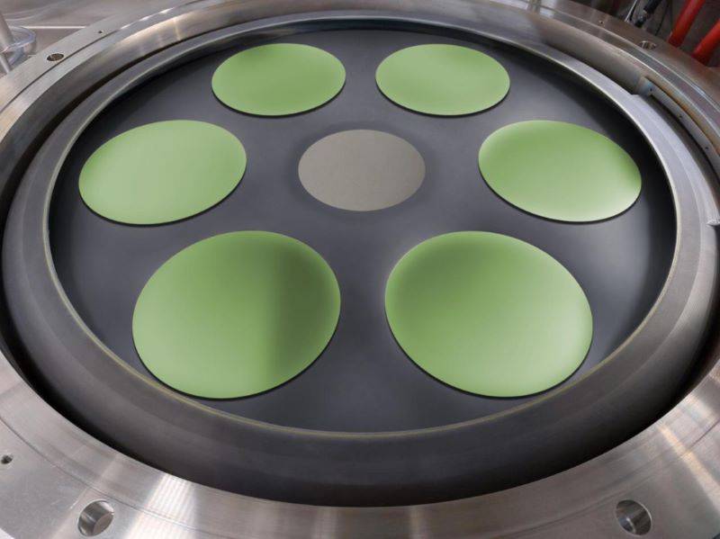
However, the challenge of mass-producing high-quality graphene with minimal defects and contaminants at a reasonable cost remains. Various methods have been developed for graphene production, each yielding different dimensions, flake shapes, and qualities. Techniques such as mechanical exfoliation, liquid-phase exfoliation, sublimation of silicon carbide (SiC), and chemical vapor deposition (CVD) have been explored. Among these, CVD has emerged as a promising method for large-scale production of uniform graphene films, as demonstrated by Li et al. in 2009.
The development of CVD technology has significantly advanced graphene synthesis, enabling large-area and mass production. By optimizing processes like batch-to-batch (B2B) and roll-to-roll (R2R), researchers have achieved increased production throughput and larger dimensions of graphene films. These advancements not only enhance the quality and scalability of graphene production but also open new avenues for its practical applications.
In summary, the rapid development of graphene preparation methods, particularly through CVD, underscores the material's vast potential and its growing importance in both scientific research and industrial applications.
Role of CVD in Graphene Applications
The Chemical Vapor Deposition (CVD) method is poised to revolutionize the landscape of graphene applications, transcending the conventional boundaries of two-dimensional films. Beyond its established role in producing high-quality graphene films, CVD is increasingly being harnessed to fabricate one-dimensional graphene ribbons and three-dimensional macro bodies, each with unique properties tailored for specific industrial and scientific needs.
CVD graphene has already made significant inroads into various technological sectors, including the design of heterostructures with semiconductors and Van der Waals heterostructures based on two-dimensional materials. This versatility extends to numerous scientific and industrial domains such as nonvolatile memories, optoelectronics, nanomechanical systems, interconnections, bioelectronics, and thermal management. Notably, graphene-based photodetectors, light-emitting diodes, and solar cells have garnered substantial interest due to their superior performance in transparent electrodes and active layers of photoelectric devices.
The scalability and adaptability of CVD make it an indispensable tool for the large-scale production of graphene. Traditional synthesis methods often fall short in terms of yield and surface area, but CVD addresses these limitations by enabling the deposition of graphene onto a variety of substrates, including transition metals like copper and nickel. These substrates can be subsequently etched to transfer graphene onto other materials, opening up new avenues for application development.
Moreover, the low sheet resistance and high optical transparency of CVD-grown graphene on copper substrates hold promise for creating advanced transparent conductive films, potentially rivaling or even surpassing traditional silicon-based technologies. As research and industrial applications continue to evolve, the role of CVD in shaping the future of graphene technology becomes increasingly pivotal, driving innovation across multiple dimensions of material science and engineering.
Related Products
- HFCVD Machine System Equipment for Drawing Die Nano-Diamond Coating
- Chemical Vapor Deposition CVD Equipment System Chamber Slide PECVD Tube Furnace with Liquid Gasifier PECVD Machine
- Microwave Plasma Chemical Vapor Deposition MPCVD Machine System Reactor for Lab and Diamond Growth
- Customer Made Versatile CVD Tube Furnace Chemical Vapor Deposition Chamber System Equipment
- Multi Heating Zones CVD Tube Furnace Machine Chemical Vapor Deposition Chamber System Equipment
Related Articles
- Understanding the CVD Diamond Machine and How It Works
- Advantages, Limitations, and Process Control of Chemical Vapor Deposition (CVD) Technology
- Chemical Vapor Deposition (CVD) and Electronic Specialty Gases
- Comprehensive Overview of CVD Inorganic Thin Film Deposition Methods
- Vapor Deposition Silicon Carbon Anode for Next-Generation Batteries


