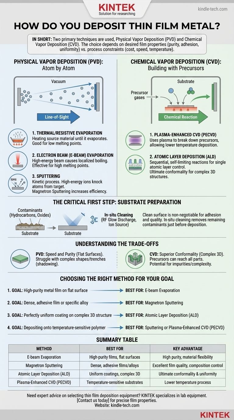
In short, thin metal films are deposited using two primary families of techniques: Physical Vapor Deposition (PVD) and Chemical Vapor Deposition (CVD). PVD methods like evaporation and sputtering physically transfer metal atoms from a source to your substrate in a vacuum, while CVD methods use chemical reactions on the substrate surface to build the film.
The choice of deposition method is not about finding the "best" technique, but about matching the right tool to the job. Your decision will be a deliberate trade-off between desired film properties—like purity, adhesion, and uniformity—and process constraints like cost, speed, and substrate temperature tolerance.
The Two Fundamental Approaches: Physical vs. Chemical
At the highest level, all deposition techniques fall into two categories based on how they deliver atoms to the surface you want to coat (the substrate). Understanding this distinction is the first step in making an informed choice.
Physical Vapor Deposition (PVD): Atom by Atom
PVD encompasses a group of processes where a material is converted into a vapor phase in a vacuum chamber and transported, atom by atom, onto a substrate where it condenses back into a thin film.
These methods are generally "line-of-sight," meaning the atoms travel in a straight line from the source to the substrate.
Common PVD Methods for Metals
Thermal/Resistive Evaporation is one of the simplest PVD methods. A current is passed through a resistive boat or filament containing the source metal, heating it until it evaporates. This method works well for metals with lower melting points.
Electron Beam (E-Beam) Evaporation is a more energetic technique. A high-energy beam of electrons is focused onto the source metal, causing localized boiling and evaporation. It is highly effective for a wide range of metals, including those with very high melting points.
Sputtering is a kinetic process, not a thermal one. High-energy ions from a plasma are accelerated into a target made of the desired metal, physically knocking atoms off its surface. These "sputtered" atoms then travel and deposit onto the substrate. Magnetron Sputtering uses magnetic fields to confine the plasma, increasing efficiency and deposition rates.
Chemical Vapor Deposition (CVD): Building with Precursors
CVD is fundamentally different. Instead of physically moving metal atoms, this process introduces volatile precursor gases into a reaction chamber.
These gases react or decompose on the heated substrate's surface, leaving behind the desired solid material as a thin film. The byproducts of the reaction are then pumped away.
Key CVD Methods
Plasma-Enhanced CVD (PECVD) uses a plasma to help break down the precursor gases. This allows deposition to occur at much lower temperatures than traditional CVD, making it suitable for temperature-sensitive substrates.
Atomic Layer Deposition (ALD) is an advanced form of CVD that offers the ultimate control. It uses a sequence of self-limiting chemical reactions to deposit a single atomic layer at a time. This provides unparalleled uniformity and the ability to perfectly coat extremely complex, three-dimensional structures.
The Critical First Step: Substrate Preparation
No deposition technique can succeed if the substrate surface is not perfectly clean. The quality and adhesion of your film depend entirely on the initial state of the surface.
Why Cleaning is Non-Negotiable
Contaminants like residual hydrocarbons, moisture, or native oxide layers act as a barrier between the substrate and the depositing film. This leads to poor adhesion, defects, and inconsistent film properties.
Common Pre-Cleaning Techniques
Before being placed in the deposition chamber, substrates are often chemically cleaned. Inside the vacuum system, further in-situ cleaning is performed. Techniques like RF glow discharge or an ion source (gridded or gridless) can be used to bombard the surface, gently sputtering away any remaining contaminants just before deposition begins.
Understanding the Trade-offs
Choosing a method requires weighing its advantages against its limitations. The ideal technique for one application may be completely wrong for another.
PVD: Speed and Purity vs. Conformality
PVD methods like evaporation and sputtering are often fast and can produce very high-purity films, especially with a good vacuum.
However, because they are line-of-sight processes, they struggle to uniformly coat complex shapes with deep trenches or undercuts. The "shadows" cast by the topography result in a much thinner or non-existent film in those areas.
CVD: Superior Conformality vs. Complexity and Purity
CVD's strength is its ability to produce highly conformal coatings. Because the precursor gases can reach every part of a complex surface, CVD and especially ALD can coat intricate 3D structures with perfect uniformity.
The trade-off is often higher process complexity and the potential for impurities. The chemical precursors themselves or reaction byproducts can sometimes be incorporated into the film, reducing its purity compared to a PVD method.
Cost, Scale, and Temperature
Simple thermal evaporation systems can be relatively inexpensive. In contrast, ALD systems represent a significant capital investment. Sputtering often provides a good balance of performance, scalability, and cost for industrial applications. Finally, the temperature tolerance of your substrate will immediately rule out high-temperature CVD processes.
Choosing the Right Method for Your Goal
Base your decision on your primary objective for the thin film.
- If your primary focus is a high-purity metal film on a flat surface: E-beam evaporation is an excellent choice for its purity and material flexibility.
- If your primary focus is a dense, adhesive film or a specific metal alloy: Magnetron sputtering is the industry standard due to its excellent film quality and control over composition.
- If your primary focus is a perfectly uniform coating on a complex 3D structure: Atomic Layer Deposition (ALD) is the superior, albeit more complex and expensive, choice.
- If your primary focus is depositing onto a temperature-sensitive polymer: Sputtering or Plasma-Enhanced CVD (PECVD) are ideal because they are lower-temperature processes.
By understanding these core principles, you can confidently select the deposition technique that aligns perfectly with your material, substrate, and performance requirements.
Summary Table:
| Method | Best For | Key Advantage |
|---|---|---|
| E-beam Evaporation | High-purity films on flat surfaces | High purity, material flexibility |
| Magnetron Sputtering | Dense, adhesive films or alloys | Excellent film quality, composition control |
| Atomic Layer Deposition (ALD) | Uniform coatings on complex 3D structures | Ultimate conformality and uniformity |
| Plasma-Enhanced CVD (PECVD) | Temperature-sensitive substrates | Lower temperature process |
Need expert advice on selecting the right thin film deposition equipment for your lab?
KINTEK specializes in lab equipment and consumables, serving all your laboratory needs. Our experts can help you choose the ideal PVD or CVD system to achieve the precise film properties—purity, adhesion, and uniformity—your research demands. Contact us today to discuss your specific application and enhance your lab's capabilities!
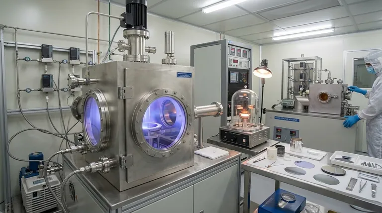
Visual Guide
Related Products
- Chemical Vapor Deposition CVD Equipment System Chamber Slide PECVD Tube Furnace with Liquid Gasifier PECVD Machine
- HFCVD Machine System Equipment for Drawing Die Nano-Diamond Coating
- Customer Made Versatile CVD Tube Furnace Chemical Vapor Deposition Chamber System Equipment
- RF PECVD System Radio Frequency Plasma-Enhanced Chemical Vapor Deposition RF PECVD
- Split Chamber CVD Tube Furnace with Vacuum Station Chemical Vapor Deposition System Equipment Machine
People Also Ask
- What happens during deposition chemistry? Building Thin Films from Gaseous Precursors
- What are the processes of vapor phase deposition? Understand CVD vs. PVD for Superior Thin Films
- How are carbon nanotubes grown? Master Scalable Production with Chemical Vapor Deposition
- What are the core advantages of PE-CVD in OLED encapsulation? Protect Sensitive Layers with Low-Temp Film Deposition
- Why is Chemical Vapor Deposition (CVD) equipment uniquely suited for constructing hierarchical superhydrophobic structures?


