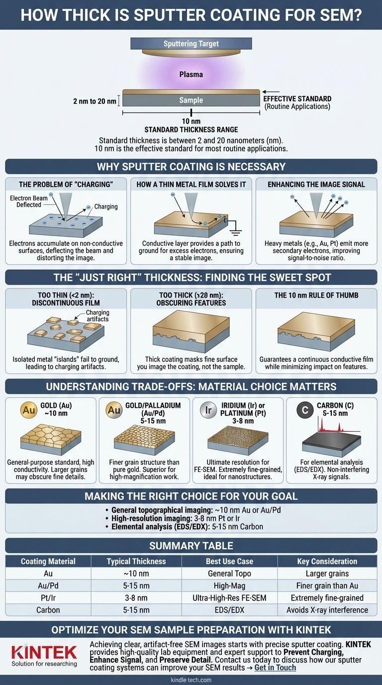
In scanning electron microscopy (SEM), the standard thickness for a sputter coating is between 2 and 20 nanometers (nm). For most routine applications, a coating of approximately 10 nm is the effective standard. This ultra-thin, electrically conductive layer is applied to non-conductive samples to prevent imaging artifacts and dramatically improve image quality.
The optimal sputter coating thickness is a balancing act. Your goal is to apply just enough conductive material—typically 2-20 nm—to prevent electron charging without obscuring the fine surface details you intend to image.
Why Sputter Coating is Necessary
To understand the importance of coating thickness, we must first understand the fundamental problem it solves: electrical charging.
The Problem of "Charging"
The SEM works by scanning a high-energy beam of electrons across a specimen. When this beam strikes a non-conductive material, the electrons accumulate on the surface because they have no path to ground.
This buildup of negative charge, known as charging, creates a localized static field that deflects the incoming electron beam. The result is a distorted, unstable image with bright patches, streaks, and a complete loss of detail.
How a Thin Metal Film Solves It
A sputter-coated layer of conductive metal forms a path for these excess electrons to dissipate. The coating is electrically connected to the metal SEM stage, which is grounded.
This continuous conductive path effectively neutralizes the sample surface, allowing the electron beam to scan without deflection and produce a stable, clear image.
Enhancing the Image Signal
Beyond preventing charging, the coating improves the image itself. Heavy metals like gold and platinum are excellent emitters of secondary electrons—the primary signal used for creating topographic images in SEM.
By coating a poor emitter with a high-yield material, you significantly increase the signal detected, resulting in a cleaner image with a much better signal-to-noise ratio.
The "Just Right" Thickness: Finding the Sweet Spot
The 2-20 nm range is not arbitrary. It represents a critical window between an ineffective coating and one that obscures your sample.
Too Thin (<2 nm): Discontinuous Film
If the coating is too thin, the deposited metal may form isolated "islands" rather than a continuous, uniform film.
These gaps in coverage fail to provide a complete path to ground. Charging can still occur in the uncoated regions, leading to persistent image artifacts.
Too Thick (>20 nm): Obscuring Features
As the coating thickness increases, it begins to mask the sample's true surface topography. The fine details you want to observe are buried under a layer of metal.
At this point, you are no longer imaging your sample; you are imaging the coating itself. This completely invalidates any analysis of surface texture or nanostructure.
The 10 nm Rule of Thumb
A 10 nm coating is a common starting point because it is thick enough to guarantee a continuous conductive film on most surfaces while being thin enough to minimize its impact on all but the very finest features.
Understanding the Trade-offs: Material Choice Matters
The ideal thickness also depends on the material you choose, which is dictated by your analytical goals.
Gold (Au): The General-Purpose Standard
Gold is popular due to its high conductivity and efficiency. However, it can form relatively large crystal grains during the coating process, which may obscure features at very high magnifications.
Gold/Palladium (Au/Pd): Finer Grain Structure
An alloy of gold and palladium produces a much finer grain structure than pure gold. This makes it a superior choice for high-magnification work where nanometer-scale details are critical.
Iridium (Ir) or Platinum (Pt): For Ultimate Resolution
For very high-resolution imaging with a Field Emission SEM (FE-SEM), materials like iridium are used. They produce an extremely fine-grained, uniform coating that is ideal for observing the smallest nanostructures, justifying their higher cost.
Carbon (C): For Elemental Analysis (EDS/EDX)
If your goal is to determine the elemental composition of your sample using Energy-Dispersive X-ray Spectroscopy (EDS or EDX), you must avoid metal coatings. The X-ray signals from a metal coat will interfere with the signals from your sample.
Carbon is the preferred choice for EDS because it is a low-atomic-number element. Its characteristic X-ray peak is very low-energy and does not conflict with the detection of other elements. A carbon coat is less conductive than metal but provides the necessary charge dissipation for analysis.
Making the Right Choice for Your Goal
Your coating strategy should be directly aligned with your imaging or analytical objective.
- If your primary focus is general topographical imaging: Start with a 10 nm gold (Au) or gold/palladium (Au/Pd) coating, which is the most reliable setup for routine work.
- If your primary focus is high-resolution imaging of fine nanostructures: Use a thinner coating (3-8 nm) of a fine-grained material like platinum (Pt) or iridium (Ir) to minimize feature obscuration.
- If your primary focus is elemental analysis (EDS/EDX): Use a carbon coating instead of metal to avoid interfering X-ray peaks, keeping it as thin as possible (5-15 nm) to ensure conductivity without absorbing the sample's X-rays.
Ultimately, selecting the correct coating thickness and material is a critical sample preparation step that directly determines the quality and accuracy of your SEM results.
Summary Table:
| Coating Material | Typical Thickness | Best Use Case | Key Consideration |
|---|---|---|---|
| Gold (Au) | ~10 nm | General topographical imaging | May have larger grains, can obscure fine details |
| Gold/Palladium (Au/Pd) | 5-15 nm | High-magnification imaging | Finer grain structure than pure gold |
| Platinum (Pt) / Iridium (Ir) | 3-8 nm | Ultra-high-resolution FE-SEM | Extremely fine-grained, ideal for nanostructures |
| Carbon (C) | 5-15 nm | Elemental analysis (EDS/EDX) | Avoids X-ray interference, less conductive |
Optimize Your SEM Sample Preparation with KINTEK
Achieving clear, artifact-free SEM images starts with precise sputter coating. KINTEK specializes in high-quality lab equipment and consumables, providing reliable sputter coaters and expert support to help you:
- Prevent Charging: Apply the perfect conductive layer (2-20 nm) to eliminate image distortion.
- Enhance Signal: Choose the right coating material (Au, Pt, C, etc.) for superior secondary electron emission.
- Preserve Detail: Balance thickness and material to avoid obscuring fine sample features.
Whether you're conducting routine imaging or advanced nanostructure analysis, KINTEK has the solutions to meet your laboratory needs. Contact us today to discuss how our sputter coating systems can improve your SEM results → Get in Touch
Visual Guide
Related Products
- Inclined Rotary Plasma Enhanced Chemical Vapor Deposition PECVD Equipment Tube Furnace Machine
- HFCVD Machine System Equipment for Drawing Die Nano-Diamond Coating
- 915MHz MPCVD Diamond Machine Microwave Plasma Chemical Vapor Deposition System Reactor
- Vacuum Hot Press Furnace Machine for Lamination and Heating
- Laboratory Sterilizer Lab Autoclave Vertical Pressure Steam Sterilizer for Liquid Crystal Display Automatic Type
People Also Ask
- What materials are deposited in PECVD? Discover the Versatile Thin-Film Materials for Your Application
- What is plasma in CVD process? Lowering Deposition Temperatures for Heat-Sensitive Materials
- What is plasma enhanced chemical vapour deposition process? Unlock Low-Temperature, High-Quality Thin Films
- What is meant by vapor deposition? A Guide to Atomic-Level Coating Technology
- What is the difference between CVD and PECVD? Choose the Right Thin-Film Deposition Method