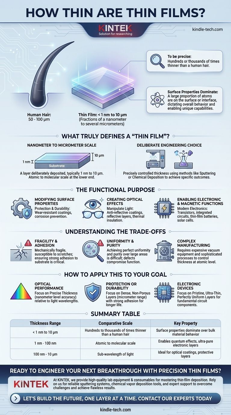
To be precise, a thin film's thickness typically ranges from fractions of a nanometer (a single layer of atoms) to several micrometers. For context, a human hair is about 50 to 100 micrometers thick, making most thin films hundreds or even thousands of times thinner. This isn't just a descriptive term; it's a specific engineering scale where the material's properties are dominated by its surface effects rather than its bulk volume.
The critical insight is that a "thin film" is defined less by a single number and more by the functional threshold where the material is so thin that its surface properties dictate its overall behavior, enabling unique optical, electrical, and protective capabilities not present in the bulk material.
What Truly Defines a "Thin Film"?
The term "thin film" refers to a specific scale of material engineering. Understanding this scale is key to grasping why these layers are so fundamental to modern technology.
The Nanometer to Micrometer Scale
A thin film is a layer of material deliberately deposited onto a substrate. Its thickness is the defining characteristic, typically falling between 1 nanometer (nm) and about 10 micrometers (µm). At the lower end, we are talking about layers that are only a few atoms thick.
When Surface Properties Dominate
In a large, bulk object, the vast majority of atoms are surrounded by other atoms, and its properties (like strength or color) are determined by this internal structure.
In a thin film, a huge proportion of the atoms are on a surface or at an interface. This is the crucial point: the physics of the surface begin to dominate the material's overall behavior. This allows for the engineering of specific properties that the bulk material simply doesn't have.
A Deliberate Engineering Choice
The thickness of a film is not arbitrary. It is precisely controlled using methods like sputtering or chemical deposition to achieve a very specific outcome. Whether for manipulating light, conducting electricity, or resisting corrosion, the exact thickness is a critical design parameter.
The Functional Purpose of Thin Films
The unique properties that emerge at this scale are the reason thin films are so widely used. The applications can be grouped by the function the film is designed to perform.
Modifying Surface Properties
The most straightforward use is to change the surface of an object. This is often done for protection or durability. Examples include hard, wear-resistant coatings on machine tools or thin layers of metal to prevent corrosion on components.
Creating Optical Effects
When a film's thickness is similar to the wavelength of light, it can manipulate how that light reflects or transmits. This is the principle behind anti-reflective coatings on eyeglasses, reflective layers on mirrors, and thermal insulation on architectural glass.
Enabling Electronic and Magnetic Functions
Modern electronics are built on thin films. In a semiconductor chip, incredibly thin and pure layers of different materials are stacked to create transistors and integrated circuits. The thinness is essential for controlling the flow of electrons over microscopic distances. Thin-film batteries and solar cells operate on similar principles.
Understanding the Trade-offs
While powerful, thin-film technology is not without its challenges. Objectivity requires acknowledging the inherent limitations.
Fragility and Adhesion
By their nature, thin films can be mechanically fragile and susceptible to scratches or damage. Furthermore, ensuring the film adheres properly to the underlying substrate is a major engineering challenge. A coating that peels off is useless.
Uniformity and Purity
Creating a film that has a perfectly uniform thickness and is free from impurities over a large area is technically difficult. Defects can compromise the film's function, whether it's an electrical short in a circuit or a visual blemish in a decorative coating.
Complex Manufacturing
The deposition processes required to create high-quality thin films are complex and often require expensive vacuum equipment. Controlling thickness at the atomic level is a highly sophisticated manufacturing task.
How to Apply This to Your Goal
The ideal thickness and properties of a thin film are entirely dependent on the problem you are trying to solve.
- If your primary focus is optical performance: The film's thickness must be precisely controlled relative to the wavelengths of light you wish to influence, often requiring nanometer-level accuracy.
- If your primary focus is protection or durability: The key is creating a dense, non-porous, and strongly adhered layer, where a greater thickness (in the micrometer range) often correlates with longer life.
- If your primary focus is electronic devices: The goal is to build pristine, ultra-thin, and perfectly uniform layers to form the fundamental components of a circuit.
Ultimately, thin-film technology is about engineering material properties at a scale where the surface becomes everything.
Summary Table:
| Thickness Range | Comparative Scale | Key Property |
|---|---|---|
| < 1 nm to 10 μm | Hundreds to thousands of times thinner than a human hair | Surface properties dominate over bulk material behavior |
| 1 nm - 100 nm | Atomic to molecular scale | Enables quantum effects, ultra-pure electronic layers |
| 100 nm - 10 μm | Sub-wavelength of light | Ideal for optical coatings, protective layers |
Ready to Engineer Your Next Breakthrough with Precision Thin Films?
At KINTEK, we specialize in providing the high-quality lab equipment and consumables you need to master thin-film deposition. Whether you are developing advanced optical coatings, durable protective layers, or next-generation electronic devices, our solutions ensure the precise thickness control, uniformity, and purity required for success.
Our target customers—research laboratories, semiconductor manufacturers, and materials science innovators—rely on KINTEK for reliable sputtering systems, chemical vapor deposition tools, and expert support to overcome the challenges of complex manufacturing and achieve flawless results.
Let's build the future, one layer at a time. Contact our experts today to discuss how KINTEK can empower your thin-film projects.
Visual Guide
Related Products
- Aluminized Ceramic Evaporation Boat for Thin Film Deposition
- Tungsten Evaporation Boat for Thin Film Deposition
- Electron Beam Evaporation Coating Oxygen-Free Copper Crucible and Evaporation Boat
- Molybdenum Tungsten Tantalum Evaporation Boat for High Temperature Applications
- Aluminum-Plastic Flexible Packaging Film for Lithium Battery Packaging
People Also Ask
- What is the source of evaporation for thin film? Choosing Between Thermal and E-Beam Methods
- What is the chemical method for thin film deposition? Build Films from the Molecular Level Up
- What is the widely used boat made of in thermal evaporation? Choosing the Right Material for High-Purity Deposition
- What are the alternatives to sputtering? Choose the Right Thin Film Deposition Method
- What are the applications of thin films deposition? Unlock New Possibilities for Your Materials


