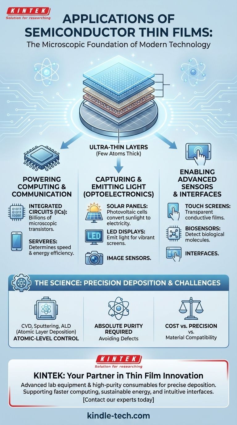
At their core, semiconductor thin films are the microscopic foundation of modern technology. They are ultra-thin layers of material, often just a few atoms thick, deposited onto a substrate like a silicon wafer. These films are the essential active components in nearly all advanced electronics, including computer hardware, mobile phones, LED displays, and solar panels, forming the basis for transistors, sensors, and photovoltaic cells.
The true significance of semiconductor thin films isn't just their use in individual products, but their role as a fundamental enabling technology. As electronic devices shrink in size and grow in power, the precision and quality of these atom-thin layers directly dictate the performance and future of the entire industry.
The Foundation of Modern Electronics
Semiconductor thin films are not merely a component; they are the functional heart of many devices. Their properties are meticulously engineered during the manufacturing process to control the flow of electricity, interact with light, and sense the environment.
Powering Computing and Communication
The most prominent application of semiconductor thin films is in the creation of integrated circuits (ICs), the "chips" that power everything from supercomputers to smartphones.
Within these chips, layers of thin films are patterned to create billions of microscopic transistors. These transistors act as digital switches, and the quality and thinness of the films determine the chip's speed and energy efficiency.
Capturing and Emitting Light
Semiconductor thin films are central to optoelectronics—the technology of light.
In solar panels, specific thin films are designed as photovoltaic cells that absorb photons from sunlight and convert that energy directly into electricity.
In LED displays, applying an electric current to different thin-film semiconductor layers causes them to emit light of specific colors, forming the vibrant images on our phone screens and televisions.
Enabling Advanced Sensors and Interfaces
The application of these films extends to how we interact with our devices and how they sense the world.
Touch screens rely on transparent conductive thin films that can register the location of a finger. Image sensors in digital cameras use thin films that convert light into electrical signals. Advanced biosensors can even use them to detect specific biological molecules.
The Science Behind the Function
The versatility of thin films comes from the ability to precisely control their properties during deposition. The chosen material and the manufacturing technique are directly related to the film's final purpose.
From Insulators to Conductors
Thin films can be engineered to be insulators, semiconductors, or conductors. By layering these materials in precise configurations, engineers build complex electronic structures like the transistor, which requires all three types of materials in close proximity.
The Critical Role of Deposition
The method used to create the film is paramount. Techniques like Chemical Vapor Deposition (CVD), sputtering, and Atomic Layer Deposition (ALD) build the film layer by layer, sometimes one atomic layer at a time.
This precision is not optional. The performance of a modern microchip is so sensitive that even a few misplaced atoms in a thin film can degrade or destroy its function.
Understanding the Trade-offs and Challenges
While semiconductor thin films are incredibly powerful, their manufacturing and implementation involve significant challenges and trade-offs.
The Pursuit of Absolute Purity
The materials used for thin films, such as precursor gases and sputtering targets, must be of exceptionally high purity. Any contamination can introduce defects that compromise the electronic or optical properties of the final device, leading to lower performance or complete failure.
Cost vs. Precision
More advanced deposition methods like ALD offer unparalleled control over thickness and uniformity, but they are often slower and more expensive than older techniques. Manufacturers must constantly balance the need for cutting-edge performance with the economic realities of mass production.
Material and Substrate Compatibility
Depositing a high-quality, crystalline thin film requires a compatible substrate. The atomic structures of the film and the surface it's grown on must align properly. This constraint drives significant research into finding the right combination of materials for new applications, such as flexible electronics or advanced batteries.
Connecting Applications to Your Core Goal
Understanding these applications helps clarify their role in different technological sectors. Your interest in semiconductor thin films likely aligns with one of three primary objectives.
- If your primary focus is computational performance: Your interest lies in the films used to create faster, smaller, and more efficient transistors within CPUs and memory chips.
- If your primary focus is energy and sustainability: Your attention should be on the photovoltaic thin films that convert sunlight into electricity and the advanced layers used in next-generation thin-film batteries.
- If your primary focus is human-device interaction: You are concerned with the transparent conductive films in touch screens and the light-emitting or light-sensing layers in modern display and camera technologies.
Ultimately, mastering the art and science of semiconductor thin films is synonymous with pushing the boundaries of what is technologically possible.
Summary Table:
| Application Area | Key Functions | Examples of Devices |
|---|---|---|
| Computing & Communication | Forming transistors for logic and memory | Microprocessors, Memory Chips, Smartphones |
| Optoelectronics | Converting light to electricity and emitting light | Solar Panels, LED Displays, Digital Cameras |
| Sensors & Interfaces | Enabling touch and detecting biological/chemical signals | Touch Screens, Biosensors, Image Sensors |
Ready to integrate high-performance semiconductor thin films into your technology?
At KINTEK, we specialize in providing the advanced lab equipment and high-purity consumables essential for developing and manufacturing these critical components. Whether your project focuses on faster computing, sustainable energy, or intuitive human-device interfaces, our expertise and products support the precise deposition and quality control required for success.
Contact our experts today to discuss how we can help you push the boundaries of your technology.
Visual Guide
Related Products
- Electron Beam Evaporation Coating Oxygen-Free Copper Crucible and Evaporation Boat
- Aluminum-Plastic Flexible Packaging Film for Lithium Battery Packaging
- Custom PTFE Wafer Holders for Lab and Semiconductor Processing
- Customizable PTFE Wafer Carriers for Semiconductor and Lab Applications
- Thin-Layer Spectral Electrolysis Electrochemical Cell
People Also Ask
- What is the voltage of e-beam evaporation? Achieve Precise Thin-Film Deposition
- What is e-beam evaporation used for? Precision Coating for Optics, Aerospace & Electronics
- How is an electron beam evaporator cooled during deposition? Essential Thermal Management for Stable Processes
- What is e-beam evaporation? Achieve High-Purity Thin Film Deposition for Your Lab
- What are the applications of electron beams? From Nanoscale Imaging to Industrial Manufacturing