At their core, thin film polymers are used to apply precise, functional coatings to surfaces. These materials are most commonly found in high-performance electronics, where they serve as insulators in semiconductor devices, and in advanced optical systems, where they are used to create specialized coatings like anti-reflective layers on lenses.
The primary value of a thin film polymer is not the material itself, but its ability to impart specific electronic or optical properties to a substrate at a microscopic scale, enabling the functionality of modern technological devices.
The Role of Thin Films in Modern Electronics
The push for smaller, more powerful, and more reliable electronics relies heavily on the unique properties of thin film polymers. They allow engineers to control electrical behavior in incredibly small spaces.
As Dielectric Insulators
In semiconductor manufacturing, layers of material must be electrically isolated from one another. Thin film polymers serve as dielectric insulators, preventing electrical current from leaking between components like transistors and capacitors.
Their high purity is critical here, as even minor impurities can compromise the insulating properties and cause device failure.
For Flexible Circuits and Displays
Unlike traditional silicon, many polymers are inherently flexible. This property is foundational for the growing field of flexible electronics, including bendable displays (OLEDs), wearable sensors, and foldable devices.
These films can be deposited on flexible substrates, allowing the entire electronic package to bend and twist without breaking the internal circuits.
In Protective Encapsulation
Sensitive electronic components are vulnerable to moisture, oxygen, and other environmental contaminants. An ultrathin polymer film can serve as a protective barrier, encapsulating the device to extend its lifespan and ensure its reliability.
Advancing Optics and Photonics
Thin film polymers give optical engineers precise control over how light interacts with a surface. By carefully layering these materials, they can filter, reflect, or transmit specific wavelengths of light.
Creating Anti-Reflective Coatings
A bare glass lens reflects a portion of the light that hits it, reducing brightness and creating glare. Applying a thin film polymer with a specific refractive index can dramatically reduce these reflections.
This is essential for applications like camera lenses, eyeglasses, solar panels, and computer displays, where maximizing light transmission is the primary goal.
Engineering Reflective Surfaces
Conversely, these films can be engineered to be highly reflective. They are used to create specialized mirrors and optical filters that reflect certain colors of light while allowing others to pass through.
Enabling Transparent Conductive Films
Some polymer films can be made both optically transparent and electrically conductive. This unique combination is the enabling technology behind touch screens, LCDs, and certain types of solar cells, where an electrical signal must pass through a clear surface.
Understanding the Trade-offs
While powerful, thin film polymers are not a universal solution. Their performance is highly dependent on a controlled and precise manufacturing process, and they come with inherent challenges.
Sensitivity to Deposition Conditions
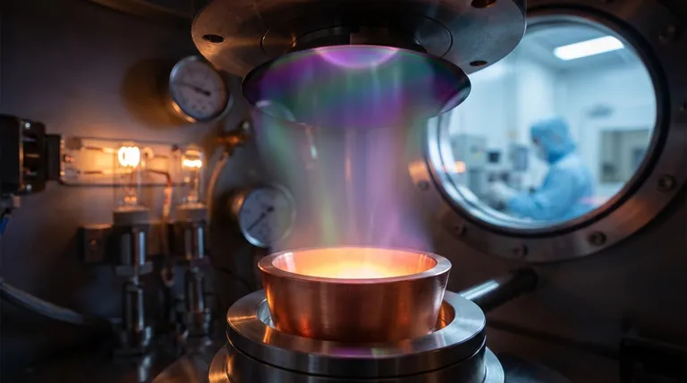
The final properties of the film are dictated by the deposition method, such as Chemical Vapor Deposition (CVD) or sputtering. Slight variations in temperature, pressure, or precursor gases during this process can lead to significant changes in film performance.
Mechanical Durability and Adhesion
Because they are exceptionally thin, these films can be susceptible to scratches, abrasion, and delamination (peeling off the substrate). Ensuring strong adhesion between the film and the surface it's coated on is a critical engineering challenge.
Purity and Defect Control
The references emphasize the use of "high purity materials" for a reason. Microscopic defects or chemical impurities can ruin the film's intended optical or electronic function, potentially leading to the failure of the entire device.
Making the Right Choice for Your Goal
The application of a thin film polymer is defined entirely by the problem you need to solve. Your design choice should be guided by the primary property you wish to achieve.
- If your primary focus is electronics manufacturing: Use thin films for their dielectric insulating properties to enable device miniaturization and protect sensitive components.
- If your primary focus is optical performance: Leverage their ability to control the refractive index of a surface to create anti-reflective or highly reflective coatings.
- If your primary focus is creating next-generation devices: Explore their use in flexible substrates and transparent conductive layers for applications like wearables and touch screens.
Ultimately, thin film polymers are a foundational tool for manipulating light and electricity at the surface level.
Summary Table:
| Application Area | Key Functions | Common Examples |
|---|---|---|
| Electronics | Dielectric insulation, flexible circuits, protective encapsulation | Semiconductors, OLED displays, wearable sensors |
| Optics & Photonics | Anti-reflective coatings, mirrors, transparent conductive films | Camera lenses, solar panels, touch screens |
Ready to integrate high-performance thin film polymers into your lab's projects? KINTEK specializes in lab equipment and consumables for advanced material deposition, including Chemical Vapor Deposition (CVD) systems. Whether you're developing next-generation electronics or precision optical coatings, our solutions ensure the purity and reliability your research demands. Contact us today to discuss how we can support your laboratory's thin film applications!
Visual Guide