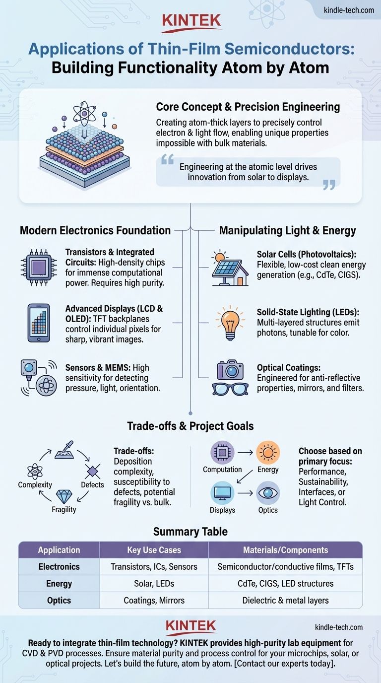
At its core, the application of thin-film semiconductors is about creating layers of material, often just atoms thick, to precisely control the flow of electrons and light. This capability makes them fundamental components in a vast range of modern technologies, from the microchips that power computation to the solar panels that generate clean energy. They are primarily used in fabricating electronic devices and creating specialized optical coatings.
The central value of thin-film semiconductors isn't just making things smaller; it's about engineering materials at the atomic level to achieve specific electronic and optical properties impossible with bulk materials. This precision is the engine driving innovation in everything from high-efficiency solar cells to next-generation displays.
The Foundation of Modern Electronics
The defining characteristic of a thin film is its microscopic thickness, which allows for the creation of compact, layered, and highly precise electronic structures. This is made possible by sophisticated manufacturing processes like Chemical Vapor Deposition (CVD) and Physical Vapor Deposition (PVD).
Transistors and Integrated Circuits
The transistors that make up a computer's processor and memory are built from many layers of thin films. Each layer of semiconductor, insulating, or conductive material is deposited with near-atomic precision.
This layering allows billions of transistors to be packed onto a single chip, enabling the immense computational power we rely on every day. The high purity of the materials used is critical to prevent defects.
Advanced Displays (LCD & OLED)
Every pixel in a modern flat-panel display, whether LCD or OLED, is controlled by at least one Thin-Film Transistor (TFT). The entire "backplane" of a screen is a massive integrated circuit made of thin films.
This technology allows each pixel to be turned on or off individually, creating the sharp, vibrant images we see on our phones, monitors, and televisions.
Sensors and MEMS
The small size and high surface-area-to-volume ratio of thin films make them ideal for sensors. They are used to detect chemicals, pressure, light, and temperature with high sensitivity.
They are also key components in Micro-Electro-Mechanical Systems (MEMS), such as the accelerometers in your phone that detect orientation.
Manipulating Light and Energy
Beyond pure electronics, thin-film semiconductors are essential for controlling and converting energy, particularly in the form of light (photons).
Solar Cells (Photovoltaics)
Thin-film solar panels are a major application. Materials like Cadmium Telluride (CdTe) or Copper Indium Gallium Selenide (CIGS) are deposited in thin layers on a substrate like glass or flexible plastic.
While sometimes less efficient than traditional silicon wafer cells, they use significantly less material, can be flexible, and often have a lower manufacturing cost, making them a vital part of the renewable energy landscape.
Solid-State Lighting (LEDs)
The light-emitting component of an LED is a multi-layered thin-film semiconductor structure. When a current is applied, electrons and "holes" combine within these specific layers, releasing energy as photons of light.
By changing the composition of these thin-film materials, manufacturers can precisely tune the color of light the LED produces.
Optical Coatings
As noted in optical systems, thin films serve a different but equally important purpose. Layers of specific materials are deposited onto lenses, mirrors, and glass.
These coatings can be engineered to be anti-reflective (like on eyeglasses), highly reflective for mirrors, or designed to filter out specific wavelengths of light for scientific instruments.
Understanding the Trade-offs
While powerful, thin-film technology is not without its challenges. The decision to use it is a classic engineering trade-off between performance, cost, and complexity.
Deposition Complexity
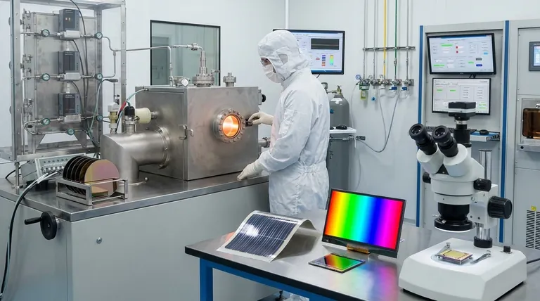
The CVD and PVD processes required to create high-quality thin films are complex and require expensive, specialized vacuum equipment. This represents a significant capital investment.
Susceptibility to Defects
Because the layers are atom-thin, a single microscopic dust particle or impurity can create a defect that ruins an entire device. This is why manufacturing must occur in ultra-clean environments with high-purity materials.
Performance vs. Durability
Thin films can be more fragile than their bulk-material counterparts. They can be prone to delamination or scratches that degrade performance, requiring protective layers or careful handling.
Making the Right Choice for Your Goal
Understanding the primary goal of your project is key to appreciating where thin-film semiconductors provide the most value.
- If your primary focus is computational performance: Your interest lies in the role of thin films in creating smaller, faster, and more power-efficient transistors for CPUs and memory chips.
- If your primary focus is energy and sustainability: The key application is in thin-film photovoltaics, which offer a path to lower-cost, flexible, and lightweight solar energy generation.
- If your primary focus is displays and interfaces: Concentrate on thin-film transistors (TFTs) as the backbone of modern OLED and LCD screens.
- If your primary focus is optical systems: The main application is in creating precision coatings for lenses, filters, and mirrors to precisely control the behavior of light.
Ultimately, mastering thin-film technology is about mastering the art of building functionality, atom by atom.
Summary Table:
| Application Area | Key Use Cases | Key Materials/Components |
|---|---|---|
| Electronics | Transistors, Integrated Circuits, Sensors, MEMS | Semiconductor & conductive thin films, TFTs |
| Energy | Solar Cells (Photovoltaics), Solid-State Lighting (LEDs) | CdTe, CIGS, multi-layer LED structures |
| Optics | Anti-reflective coatings, Highly reflective mirrors, Optical filters | Precision-deposited dielectric & metal layers |
Ready to integrate thin-film technology into your project?
At KINTEK, we specialize in providing the high-purity lab equipment and consumables essential for precise thin-film deposition processes like CVD and PVD. Whether you are developing advanced microchips, next-generation solar panels, or high-performance optical coatings, our solutions ensure the material purity and process control you need for success.
Let's build the future, atom by atom. Contact our experts today to discuss your specific laboratory requirements.
Visual Guide
Related Products
- Customizable PTFE Wafer Carriers for Semiconductor and Lab Applications
- Custom PTFE Wafer Holders for Lab and Semiconductor Processing
- Thin-Layer Spectral Electrolysis Electrochemical Cell
- Aluminum-Plastic Flexible Packaging Film for Lithium Battery Packaging
People Also Ask
- What are the technical advantages of using PTFE laboratory consumables? Ensure Ultimate Chemical Resistance
- How is PTFE utilized for insulation in Alloy 22 corrosion setups? Ensure Signal Purity & Accuracy
- Why is PTFE wire used for hanging metal specimens in biodiesel corrosion tests? Ensure Pure Experimental Results
- Why are PTFE containers required for PCT leaching tests? Ensure Chemical Inertness and Analytical Precision
- Why is slender PTFE tubing necessary for flow control in multi-channel catalyst aging? Ensure Equal Gas Distribution