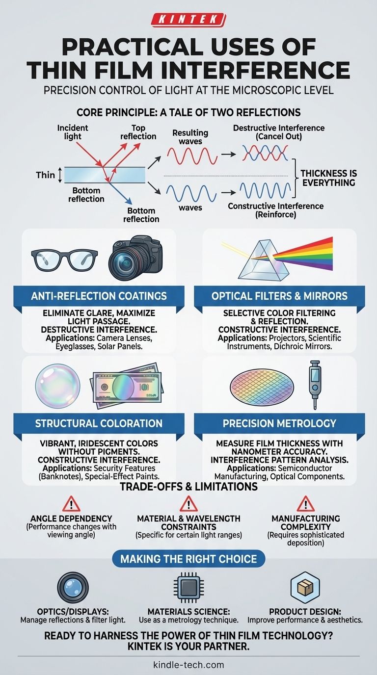
In essence, thin film interference is a fundamental principle used to precisely control light. Its most common applications include the anti-reflection coatings on your eyeglasses and camera lenses, the selective color filters in optical instruments, and even the iridescent security features on banknotes. This phenomenon occurs when light waves reflecting off the top and bottom surfaces of a transparent, microscopic layer either cancel each other out or reinforce each other.
The core takeaway is not simply about creating colors or reducing glare. It's about using a film's precisely engineered thickness—often just a few nanometers—to selectively eliminate or amplify specific wavelengths of light. This ability to manipulate light at a microscopic level is the foundation for enhancing optical performance in countless technologies.
How a Microscopic Layer Controls Light
To grasp the applications, you first need to understand the underlying mechanism. The effect is entirely dependent on how light waves interact with each other after reflecting from a thin film.
The Core Principle: A Tale of Two Reflections
When light hits a thin film, such as the coating on a lens, some of it reflects off the top surface. The rest of the light enters the film, travels through it, and reflects off the bottom surface.
You now have two separate reflected light waves. The wave that traveled through the film has taken a slightly longer path, causing it to be out of sync with the first wave that reflected from the top surface.
Constructive vs. Destructive Interference
This "out-of-sync" relationship is the key.
- Destructive interference occurs when the peaks of one reflected wave align with the troughs of the other, causing them to cancel each other out. This is the goal of anti-reflection coatings.
- Constructive interference occurs when the peaks of both waves align, reinforcing each other and making a specific color (wavelength) appear brighter. This is responsible for the vibrant colors on a soap bubble.
Thickness is Everything
The critical factor that determines whether interference is constructive or destructive is the thickness of the film. Engineers can precisely deposit a film of a specific thickness to target and control a desired wavelength of light.
Key Applications in Modern Technology
This simple principle of controlling wave interactions enables some of our most advanced optical technologies.
Anti-Reflection Coatings (The "Invisible" Film)
This is the most widespread commercial use of thin film interference. A coating is applied that is exactly the right thickness to cause reflected visible light waves to cancel each other out.
This destructive interference prevents glare and maximizes the amount of light that passes through the surface. You find this on camera lenses, eyeglasses, microscope optics, and the surface of solar panels to improve efficiency.
Optical Filters and Mirrors (Selective Vision)
By stacking multiple thin films of varying thicknesses, engineers can create highly specialized filters. These devices use constructive interference to reflect unwanted wavelengths while allowing desired wavelengths to pass through.
These "dichroic" filters are used in projection systems to separate red, green, and blue light, and in scientific instruments to isolate specific spectral lines for analysis.
Structural Coloration (Engineering with Light)
Unlike pigments which absorb light, structural color is produced when a microscopic structure—like a thin film—causes light waves to interfere. The shimmering colors on a soap bubble or an oil slick are classic examples.
This principle is used commercially to create special-effect paints for cars and security features on currency and passports that change color as you tilt them.
Precision Metrology (Using Light as a Ruler)
In high-tech manufacturing, especially for semiconductors and optical components, ensuring the thickness of deposited films is perfect is critical.
By shining light on a coated surface, technicians can analyze the interference pattern of the reflected light. The peaks and valleys in the resulting spectrum act as a precise ruler, allowing them to measure film thickness with nanometer-level accuracy.
Understanding the Trade-offs and Limitations
While powerful, thin film interference is not a perfect solution for all scenarios. Its effectiveness is governed by specific physical constraints.
Angle Dependency
The performance of an interference coating is optimized for a specific angle of light incidence (usually straight on). If you view the surface from a sharp angle, the path length difference for the light changes, altering the interference effect. This is why you might see a faint colored sheen when you look at coated eyeglasses from the side.
Material and Wavelength Constraints
The choice of coating material and its refractive index is tightly coupled to the target wavelengths. A coating designed to be anti-reflective for visible light will not perform the same way for ultraviolet or infrared light. Designing broadband coatings that work across a wide spectrum requires complex and expensive multi-layer designs.
Manufacturing Complexity
Depositing a film with uniform thickness at the nanometer scale over a large surface is a significant engineering challenge. It requires sophisticated vacuum deposition equipment and cleanroom environments, which contributes to the cost of high-performance optical components.
Making the Right Choice for Your Goal
Understanding this principle allows you to recognize its impact across various fields and leverage it for specific outcomes.
- If your primary focus is on optics or displays: Think of interference as your primary tool for managing reflections, filtering light, and enhancing visual clarity and device efficiency.
- If your primary focus is on materials science or manufacturing: Recognize interference as a critical metrology technique for guaranteeing nanometer-scale precision in thin film deposition processes.
- If your primary focus is on product design: Leverage interference coatings as a functional finish to improve performance, whether by increasing the energy output of a solar cell or reducing distracting glare on a user interface.
By engineering these microscopic layers with precision, we gain macroscopic control over the fundamental behavior of light itself.
Summary Table:
| Application | Key Function | Principle Used |
|---|---|---|
| Anti-Reflection Coatings | Eliminate glare on lenses, glasses, and solar panels | Destructive Interference |
| Optical Filters & Mirrors | Selectively transmit or reflect specific light wavelengths | Constructive Interference |
| Structural Coloration | Create vibrant, iridescent colors for security and design | Constructive Interference |
| Precision Metrology | Measure film thickness with nanometer accuracy | Interference Pattern Analysis |
Ready to harness the power of thin film technology in your lab? Whether you need to develop advanced optical coatings, require precise metrology for your manufacturing process, or are sourcing high-quality lab equipment for thin film research, KINTEK is your partner. We specialize in providing the laboratory equipment and consumables that enable precision and innovation. Contact our experts today to discuss how we can support your specific application needs.
Visual Guide