At its core, Chemical Vapor Deposition (CVD) is a multi-step process for creating a high-quality, solid thin film on a substrate from gaseous reactants. The essential sequence involves transporting reactive gases to the substrate, where they adsorb onto the surface, undergo a chemical reaction to form the film, and finally, the gaseous by-products of this reaction are removed. This controlled, bottom-up assembly allows for the creation of exceptionally pure and dense coatings.
The fundamental principle of CVD is a controlled chemical reaction on a heated surface. Precursor gases are introduced into a chamber, where they decompose and react on a substrate to build a solid film one layer of atoms at a time, making it a powerful tool for manufacturing advanced materials.
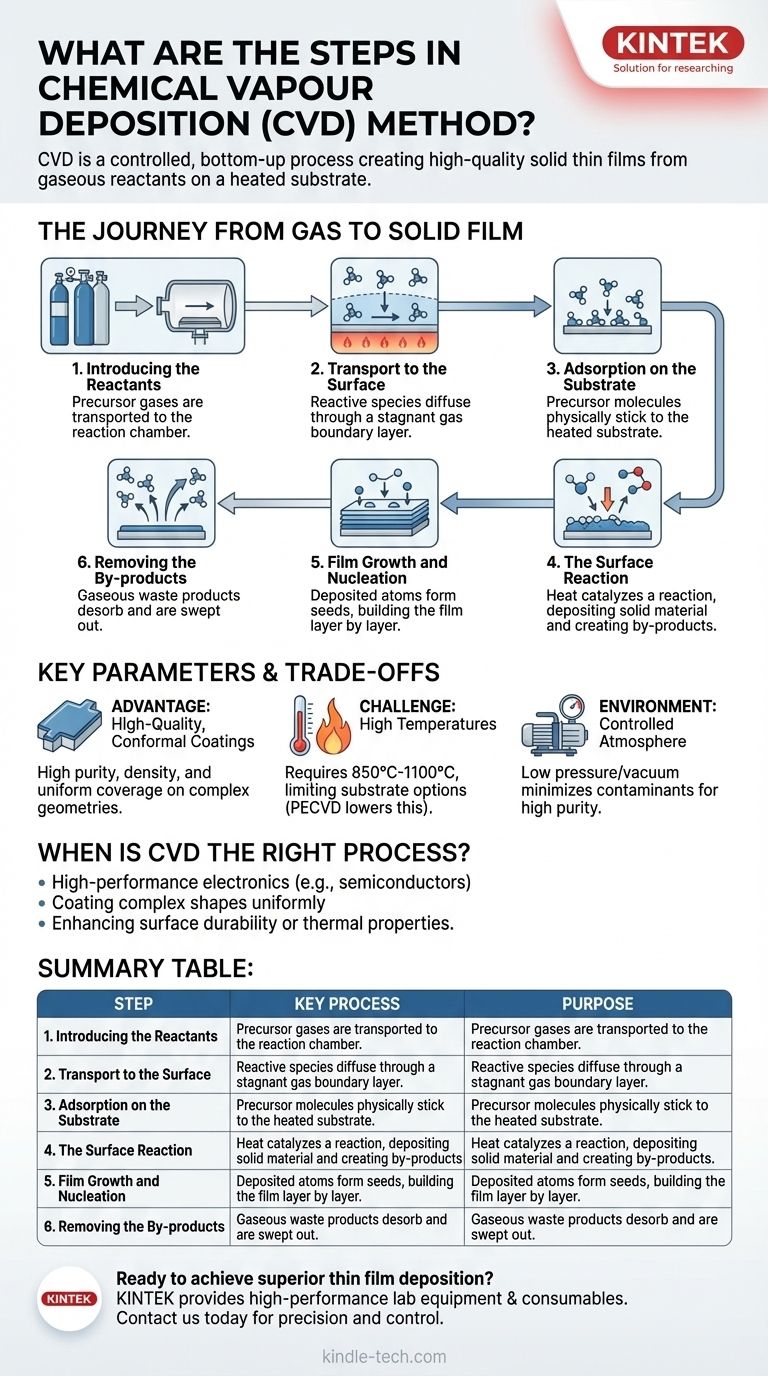
The Journey from Gas to Solid Film
Understanding CVD requires following the path of precursor molecules as they transform from a gas into a precise, solid layer. The entire process takes place under carefully controlled conditions of temperature and low pressure, often in a vacuum, to ensure purity and prevent unwanted reactions.
Step 1: Introducing the Reactants
The process begins by introducing one or more volatile precursor gases into the reaction chamber. These gases contain the elements that will ultimately form the final film. They are transported towards the substrate through convection and diffusion.
Step 2: Transport to the Surface
As the gases approach the heated substrate, a thin, stagnant layer of gas known as the boundary layer forms just above the surface. The reactive species must diffuse through this layer to reach the substrate, a step that can influence the uniformity and growth rate of the film.
Step 3: Adsorption on the Substrate
Once the precursor gas molecules reach the substrate, they physically stick to the surface in a process called adsorption. This is a critical prerequisite for the chemical reaction; the molecules must be temporarily held on the surface to react.
Step 4: The Surface Reaction
This is the central step of CVD. The energy provided by the heated substrate catalyzes a heterogeneous chemical reaction among the adsorbed molecules. This reaction breaks down the precursors, depositing the desired solid material and creating volatile by-products.
Step 5: Film Growth and Nucleation
The deposited atoms act as nucleation sites, or seeds, for further growth. Other atoms diffusing across the surface will find these sites and bond to them, gradually building up the film layer by layer to form a continuous, crystalline, or amorphous coating.
Step 6: Removing the By-products
The chemical reaction creates gaseous waste products that are no longer needed. These by-products desorb (detach) from the substrate surface, diffuse back out through the boundary layer, and are then swept out of the reaction chamber by the gas flow.
Understanding the Key Parameters and Trade-offs
While powerful, CVD is not a universal solution. Its effectiveness is governed by a balance of its unique advantages and inherent limitations, which dictates where it is best applied.
The Advantage: High-Quality, Conformal Coatings
CVD is renowned for producing films of high purity and density. Because it builds the film atom by atom, it offers exceptional control over the material's chemical composition, crystal structure, and thickness. A key benefit is its ability to create conformal coatings that uniformly cover complex, three-dimensional shapes.
The Challenge: High Temperatures
The primary limitation of traditional CVD is the high reaction temperature, often between 850°C and 1100°C. Many substrate materials cannot withstand this heat without melting or degrading. However, modern variations like Plasma-Enhanced CVD (PECVD) can significantly lower this temperature requirement.
The Environment: The Need for Controlled Atmosphere
The process must occur under low atmospheric pressure or vacuum to minimize contaminants and background gases. This ensures that the only reactions taking place are the intended ones, leading to the high purity of the final film. This requirement adds to the complexity and cost of the equipment.
When is CVD the Right Process?
Choosing CVD depends entirely on the required properties of the final film. The process excels where quality and precision are more important than cost or processing temperature.
- If your primary focus is high-performance electronics or sensors: CVD is the leading method for creating high-quality, low-defect graphene and other advanced semiconductor layers.
- If your primary focus is coating complex shapes uniformly: CVD's "wrap-around" capability makes it ideal for components with intricate geometries that other line-of-sight methods cannot cover.
- If your primary focus is enhancing surface durability or thermal properties: CVD is used to apply extremely hard and resilient coatings, such as ceramics or alloys, to improve the performance of underlying materials.
Ultimately, Chemical Vapor Deposition is a foundational technology for building advanced materials from the molecular level up.
Summary Table:
| Step | Key Process | Purpose |
|---|---|---|
| 1 | Introducing Reactants | Deliver precursor gases to the reaction chamber. |
| 2 | Transport to Surface | Gases diffuse through a boundary layer to reach the substrate. |
| 3 | Adsorption | Precursor molecules physically stick to the substrate surface. |
| 4 | Surface Reaction | Heat catalyzes a reaction, depositing the solid film material. |
| 5 | Film Growth & Nucleation | Deposited atoms build the film layer by layer. |
| 6 | Removing By-products | Gaseous waste products are desorbed and swept from the chamber. |
Ready to achieve superior thin film deposition in your lab?
KINTEK specializes in providing high-performance lab equipment and consumables for advanced processes like Chemical Vapor Deposition. Whether you are developing high-performance electronics, coating complex components, or enhancing material durability, our solutions are designed to deliver the precision, purity, and control your research demands.
Contact us today to discuss how our expertise can support your specific laboratory needs and help you build advanced materials from the molecular level up.
Visual Guide
Related Products
- Chemical Vapor Deposition CVD Equipment System Chamber Slide PECVD Tube Furnace with Liquid Gasifier PECVD Machine
- RF PECVD System Radio Frequency Plasma-Enhanced Chemical Vapor Deposition RF PECVD
- Microwave Plasma Chemical Vapor Deposition MPCVD Machine System Reactor for Lab and Diamond Growth
- Customer Made Versatile CVD Tube Furnace Chemical Vapor Deposition Chamber System Equipment
- 915MHz MPCVD Diamond Machine Microwave Plasma Chemical Vapor Deposition System Reactor
People Also Ask
- What are the processes of vapor phase deposition? Understand CVD vs. PVD for Superior Thin Films
- How expensive is chemical vapor deposition? Understanding the True Cost of High-Performance Coating
- Why is Chemical Vapor Deposition (CVD) equipment uniquely suited for constructing hierarchical superhydrophobic structures?
- What is the chemical vapor deposition growth process? Build Superior Thin Films from the Atom Up
- What happens during deposition chemistry? Building Thin Films from Gaseous Precursors


