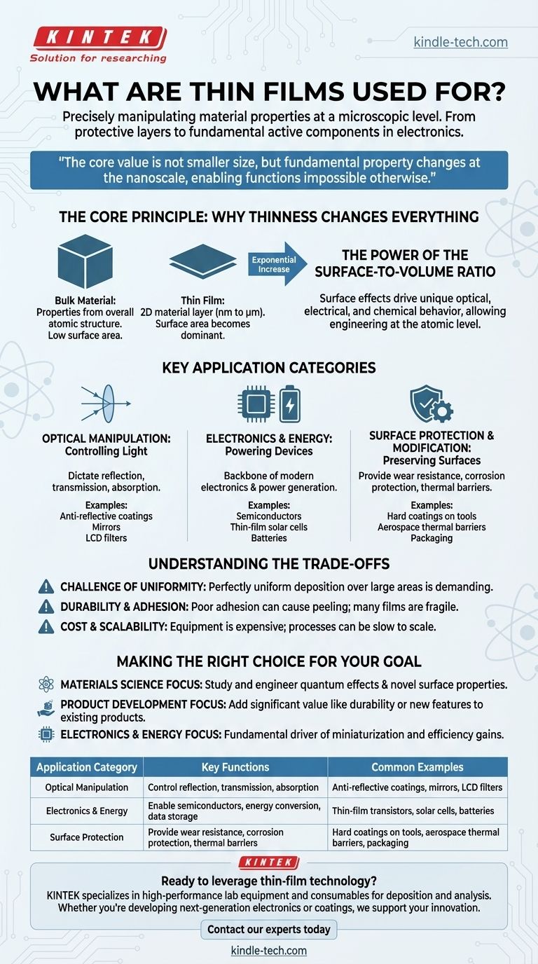
In essence, thin films are used to precisely manipulate material properties at a microscopic level. They serve as everything from protective anti-corrosion layers and optical anti-reflection coatings on glasses to the fundamental active layers in semiconductors, solar cells, and digital displays. Their applications span nearly every modern industry by allowing engineers to give a material new optical, electrical, or physical characteristics that its bulk form does not possess.
The core value of a thin film is not that it's a smaller version of a material, but that its properties fundamentally change at the nanoscale. This allows us to engineer materials with specific functions—like controlling light, conducting electricity, or resisting wear—that are impossible to achieve otherwise.
The Core Principle: Why Thinness Changes Everything
To understand the vast applications of thin films, you must first grasp why reducing a material's thickness from millimeters to nanometers changes its behavior so dramatically.
From Bulk Material to Thin Film
A bulk material, like a block of metal or glass, has properties determined by its overall atomic structure. Its surface area is tiny compared to its total volume.
A thin film, by contrast, is a layer of material ranging from a few nanometers to several micrometers in thickness. At this scale, the surface becomes a dominant factor.
The Power of the Surface-to-Volume Ratio
As you make a material thinner, its surface-to-volume ratio increases exponentially. This means a much higher percentage of its atoms are at the surface, interacting with the environment.
This change is the source of a thin film's unique properties. Surface effects, which are negligible in bulk materials, become the primary drivers of the film's optical, electrical, and chemical behavior.
Engineering Properties at the Atomic Level
Creating a thin film allows us to build structures layer by atomic layer. We can precisely control thickness, composition, and crystal structure to "dial in" desired properties.
For example, a film's thickness can be engineered to be a quarter of the wavelength of light, creating an anti-reflective coating. This level of precision is the key to its power.
Key Application Categories Explained
The unique properties of thin films are exploited across several major industrial domains.
Optical Manipulation: Controlling Light
Many of the most common applications involve manipulating light. By controlling a film's thickness and refractive index, we can dictate how it reflects, transmits, or absorbs light waves.
This is the principle behind anti-reflective coatings on eyeglasses, mirrors on telescopes, thermal insulation on architectural glass, and color filters in light crystal displays (LCDs).
Electronics and Energy: Powering Modern Devices
Thin films are the backbone of the modern electronics industry. The entire field of semiconductors relies on depositing multiple thin layers of different materials to create the microscopic transistors that power our computers.
Similarly, thin-film solar cells convert light to electricity, magnetic storage media uses thin magnetic layers to store data, and next-generation thin-film batteries promise higher energy density in smaller packages.
Surface Protection and Modification
One of the simplest yet most critical uses is to protect a surface. A thin, hard film can provide wear protection on cutting tools, while a chemically inert film can prevent corrosion on metal parts.
In aerospace, specialized thin films act as thermal barriers to protect components from extreme heat. Even the metallic foil in food packaging is a thin film designed to preserve freshness.
Understanding the Trade-offs
While powerful, thin-film technology is not without its challenges. Objectivity requires acknowledging its limitations.
The Challenge of Uniformity
Depositing a perfectly uniform film, especially over a large area, is technically demanding. Any variation in thickness can degrade performance, whether it's an optical coating with inconsistent color or a semiconductor with faulty circuits.
Durability and Adhesion
A thin film is only as good as its ability to stick to the underlying material (the substrate). Poor adhesion can cause films to peel, crack, or delaminate, rendering the device useless. Many films are also inherently fragile and susceptible to scratching.
Cost and Scalability
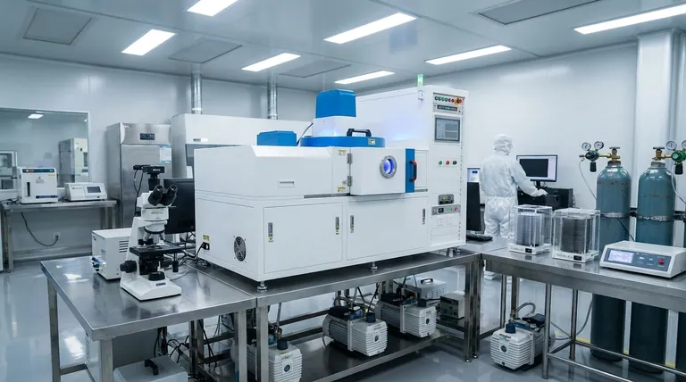
The equipment used for thin-film deposition, such as sputtering or chemical vapor deposition systems, can be extremely expensive. The processes can also be slow, making it a challenge to scale production for certain high-precision applications affordably.
Making the Right Choice for Your Goal
Understanding the purpose of thin films allows you to see them not just as a component, but as a strategic tool for engineering.
- If your primary focus is materials science: Thin films are the primary vehicle for studying and engineering quantum effects and novel surface properties.
- If your primary focus is product development: A thin-film coating is a key method for adding significant value, such as durability, new optical features, or electrical functionality, to an existing product.
- If your primary focus is electronics or energy: Thin-film technology is the fundamental driver of miniaturization and efficiency gains in semiconductors, displays, and solar cells.
By mastering the properties of materials at their thinnest, we unlock capabilities that define modern technology.
Summary Table:
| Application Category | Key Functions | Common Examples |
|---|---|---|
| Optical Manipulation | Control reflection, transmission, and absorption of light | Anti-reflective coatings, mirrors, LCD filters |
| Electronics & Energy | Enable semiconductors, energy conversion, and data storage | Thin-film transistors, solar cells, batteries |
| Surface Protection | Provide wear resistance, corrosion protection, and thermal barriers | Hard coatings on tools, aerospace thermal barriers, packaging |
Ready to leverage thin-film technology for your lab or product? KINTEK specializes in high-performance lab equipment and consumables for thin-film deposition and analysis. Whether you're developing next-generation semiconductors, optical coatings, or protective layers, our solutions help you achieve precise, reliable results. Contact our experts today to discuss how we can support your thin-film innovation!
Visual Guide
Related Products
- Aluminized Ceramic Evaporation Boat for Thin Film Deposition
- Tungsten Evaporation Boat for Thin Film Deposition
- Electron Beam Evaporation Coating Oxygen-Free Copper Crucible and Evaporation Boat
- Aluminum-Plastic Flexible Packaging Film for Lithium Battery Packaging
- Thin-Layer Spectral Electrolysis Electrochemical Cell
People Also Ask
- What is the source of evaporation for thin film? Choosing Between Thermal and E-Beam Methods
- Why is an alumina boat selected for catalyst precursors? Ensure Sample Purity at 1000 °C
- Why is an alumina boat and Ti3AlC2 powder bed necessary for Ti2AlC sintering? Protect MAX Phase Purity
- What is the chemical method for thin film deposition? Build Films from the Molecular Level Up
- What are the applications of thin films deposition? Unlock New Possibilities for Your Materials


