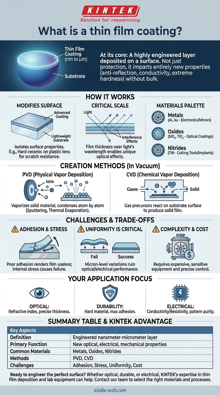
At its core, a thin film coating is an extremely thin layer of material, ranging from a few atoms (nanometers) to a few thousand atoms (micrometers) thick, that is deposited onto the surface of an object, known as a substrate. This process is not like painting; it's a precise engineering technique designed to give the substrate’s surface entirely new properties—such as anti-reflection, electrical conductivity, or extreme hardness—that the bulk material does not possess on its own.
The crucial concept to grasp is that thin film coatings are not merely protective layers. They are highly engineered, functional surfaces that fundamentally change how an object interacts with light, electricity, heat, or physical force.
How a Thin Film Fundamentally Works
The power of a thin film comes from its ability to add new functionality without changing the core structure or properties of the underlying object.
Modifying the Surface, Not the Bulk
A thin film isolates the surface properties from the bulk properties of a material. This allows you to use a substrate that is strong, lightweight, or inexpensive (like plastic or glass) and apply a coating that gives its surface an advanced optical, electrical, or mechanical characteristic.
For example, a plastic lens is lightweight and shatter-resistant, but it scratches easily. A micro-thin layer of a hard, transparent ceramic coating gives it the scratch resistance it needs without adding any perceptible weight or thickness.
The Critical Importance of Scale
The "thinness" of the film is what enables its unique capabilities. When a film's thickness is close to the wavelength of light, it can create interference effects. This is the principle behind anti-reflection coatings on eyeglasses, which use precisely layered films to cancel out reflected light waves.
At this scale, the properties of a material can be different from its bulk form, enabling effects that are impossible to achieve with thicker materials.
A Vast Palette of Materials
Thin films can be created from a wide range of materials, each chosen for a specific function:
- Metals (e.g., aluminum, gold): Used for reflective coatings on mirrors or conductive pathways in electronics.
- Oxides (e.g., silicon dioxide, titanium dioxide): Commonly used in optical coatings for their transparency and specific refractive indices.
- Nitrides (e.g., titanium nitride): Valued for their extreme hardness and wear resistance, often used on cutting tools and medical implants.
Key Methods of Creating Thin Films
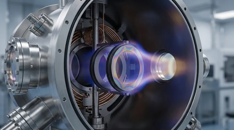
Applying a layer of material that is only a few hundred atoms thick requires highly controlled processes, typically performed in a vacuum.
Physical Vapor Deposition (PVD)
PVD encompasses a set of methods where a solid material is vaporized in a vacuum and condenses onto the substrate, atom by atom. Think of it as a form of atomic "spray painting." Common PVD methods include sputtering, where a target is bombarded with ions to eject atoms, and thermal evaporation, where a material is heated until it vaporizes.
Chemical Vapor Deposition (CVD)
In CVD, the substrate is exposed to one or more volatile precursor gases. These gases react or decompose on the substrate's surface to produce the desired solid thin film. It's analogous to how dew forms on a cool surface, but in this case, the "dew" is a permanent, solid, and highly engineered layer.
Understanding the Trade-offs and Challenges
While incredibly powerful, thin film technology involves significant engineering challenges that dictate its application and cost.
Adhesion and Internal Stress
The single most critical factor for a coating is that it sticks to the substrate. Poor adhesion renders the film useless. Furthermore, as the film is deposited, internal stress can build up, which can cause the film to crack or peel away over time, especially when subjected to temperature changes.
Uniformity is Critical
For most applications, especially in optics and semiconductors, the film's thickness must be perfectly uniform across the entire surface. Even minuscule variations—measured in angstroms—can ruin the performance of the device by altering its optical or electrical properties.
Process Complexity and Cost
The equipment required for thin film deposition (like vacuum chambers and high-purity material sources) is complex and expensive. The processes are sensitive to contamination and require precise control, making high-performance coatings a significant investment.
How to Think About Thin Films for Your Application
Your goal determines which material and process characteristics are most important.
- If your primary focus is optical performance: The key factors are the material's refractive index and maintaining precise thickness control to create the desired interference effects.
- If your primary focus is durability and protection: The priority is selecting a hard material (like a nitride or diamond-like carbon) and ensuring the deposition process achieves maximum adhesion to the substrate.
- If your primary focus is electrical functionality: The choice of material is based on its conductivity or resistivity, and the process must ensure the film is pure and patterned correctly without defects.
Ultimately, understanding thin films is realizing that a material's most critical and valuable interactions often happen right at its surface.
Summary Table:
| Key Aspect | Description |
|---|---|
| Definition | A highly engineered layer (nanometers to micrometers thick) deposited on a substrate. |
| Primary Function | Imparts new optical, electrical, or mechanical properties to the surface. |
| Common Materials | Metals (Al, Au), Oxides (SiO₂, TiO₂), Nitrides (TiN). |
| Deposition Methods | Physical Vapor Deposition (PVD), Chemical Vapor Deposition (CVD). |
| Key Challenges | Adhesion, internal stress, thickness uniformity, process cost. |
Ready to engineer the perfect surface for your application? Whether your priority is optical performance, extreme durability, or electrical functionality, KINTEK's expertise in thin film deposition and lab equipment can help you achieve it. Our specialists will work with you to select the right materials and processes for your substrate. Contact our team today to discuss your project and discover the KINTEK advantage in precision coatings.
Visual Guide
Related Products
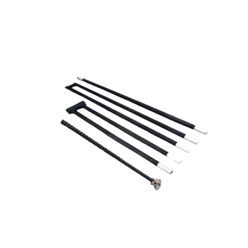
- Custom CVD Diamond Coating for Lab Applications
- RF PECVD System Radio Frequency Plasma-Enhanced Chemical Vapor Deposition RF PECVD
- Customer Made Versatile CVD Tube Furnace Chemical Vapor Deposition Chamber System Equipment
- 1200℃ Split Tube Furnace with Quartz Tube Laboratory Tubular Furnace
- Vacuum Hot Press Furnace Machine for Lamination and Heating
People Also Ask
- What are diamond coated films? Enhance Materials with Super-Hard, Transparent Layers
- How thick is CVD diamond coating? Balancing Durability and Stress for Optimal Performance
- How are tools coated with diamond? Achieve Superior Hardness and Low Friction for Your Tools
- Is diamond coating worth it? Maximize Component Life and Performance
- Is diamond coating permanent? The Truth About Its Long-Lasting Durability