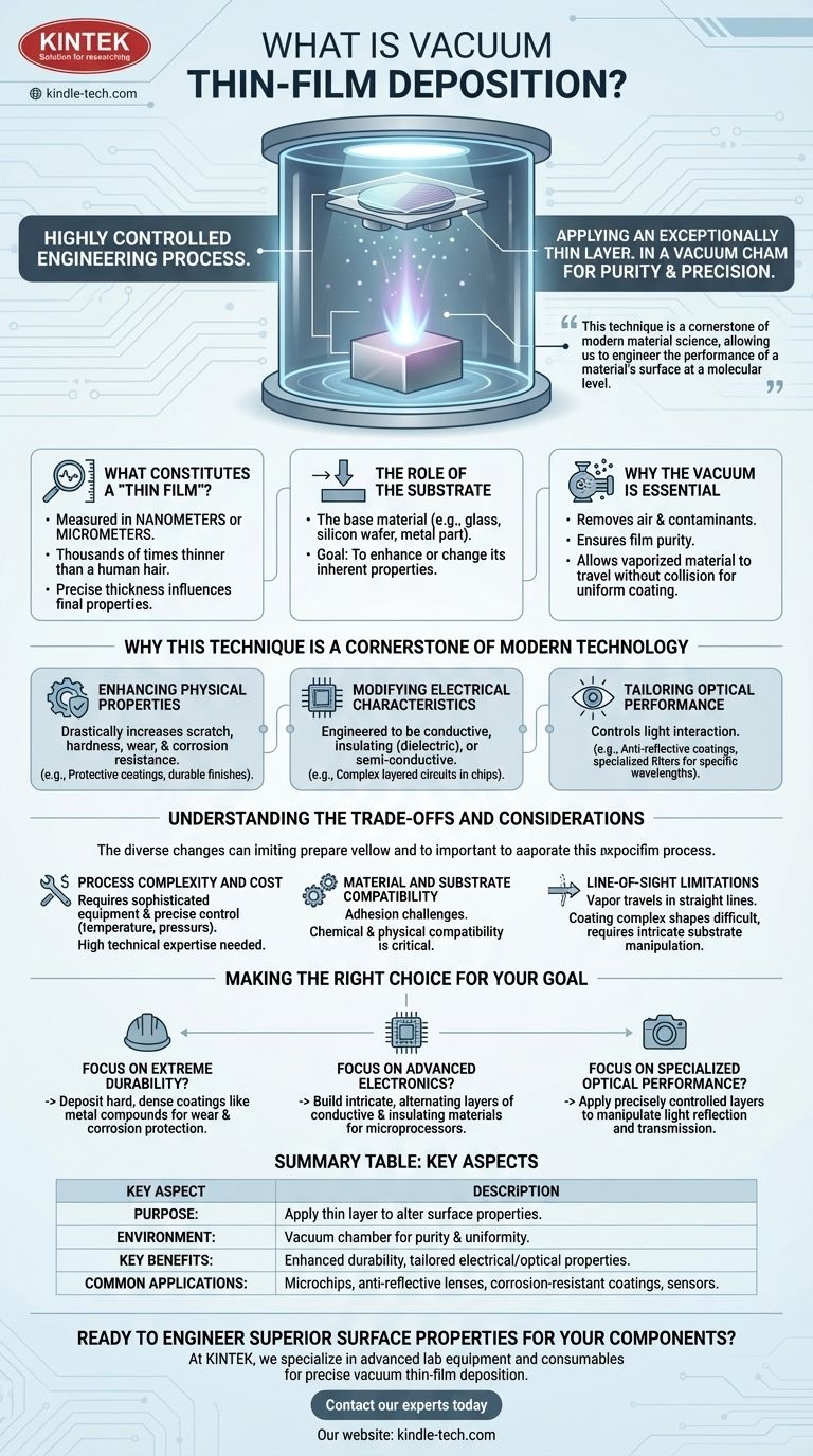
In essence, vacuum thin-film deposition is a highly controlled engineering process for applying an exceptionally thin layer of one material onto the surface of another, known as a substrate. This entire operation takes place inside a vacuum chamber to ensure purity and precision. The purpose is not merely to coat an object, but to fundamentally alter its surface properties, granting it new capabilities like extreme durability, electrical insulation, or specific optical characteristics.
This technique is a cornerstone of modern material science, allowing us to engineer the performance of a material's surface at a molecular level. It's how we create everything from the anti-glare screen on your smartphone to the corrosion-resistant coatings on aerospace components.
The Core Principles of the Process
To understand the value of this technique, it's essential to break down its core components: the film, the substrate, and the vacuum environment itself.
What Constitutes a "Thin Film"?
A "thin film" is a layer of material whose thickness is measured in nanometers or micrometers. To put this in perspective, these layers can be thousands of times thinner than a single human hair.
The precise thickness is critical, as it directly influences the final properties of the component.
The Role of the Substrate
The substrate is simply the base material or component onto which the thin film is applied. This could be a piece of glass for a camera lens, a silicon wafer for a microchip, or a metal part for a medical implant.
The goal of the deposition is to enhance or change the inherent properties of this substrate.
Why the Vacuum is Essential
Conducting the process in a vacuum is non-negotiable for achieving a high-quality film. The vacuum chamber removes air, water vapor, and other particle contaminants.
This pristine environment ensures two things: first, the deposited film remains pure, and second, the vaporized coating material can travel from its source to the substrate without colliding with other molecules, resulting in a uniform and strongly bonded layer.
Why This Technique is a Cornerstone of Modern Technology
Thin-film deposition is not a niche process; it is a foundational manufacturing technique that enables countless modern technologies by precisely tailoring surface characteristics.
Enhancing Physical Properties
One of the most common applications is to improve a substrate's physical durability. By depositing layers of hard materials like metals or ceramics, we can drastically increase scratch resistance, hardness, wear, and corrosion resistance.
This is used for everything from protective coatings on cutting tools to durable finishes on automotive parts.
Modifying Electrical Characteristics
The process is vital to the electronics industry. Thin films can be engineered to be electrically conductive, insulating (dielectric), or semi-conductive.
This allows for the creation of the complex, microscopic layered circuits found in all modern computer chips and electronic devices.
Tailoring Optical Performance
Thin films are used to control how light interacts with a surface. By applying layers with specific thicknesses and refractive indices, we can create anti-reflective coatings for eyeglasses and camera lenses or specialized filters that transmit or block specific wavelengths of light.
Understanding the Trade-offs and Considerations
While incredibly powerful, vacuum thin-film deposition is a complex process with inherent challenges that must be managed.
Process Complexity and Cost
This is not a simple coating method. It requires sophisticated and expensive vacuum equipment, along with precise control over variables like temperature, pressure, and deposition rate.
Achieving a consistent, high-quality result demands significant technical expertise and investment.
Material and Substrate Compatibility
Not all materials are suitable for deposition, and ensuring the thin film properly adheres to the substrate is a common engineering challenge. The chemical and physical compatibility between the film and the substrate is critical for a successful and durable coating.
Line-of-Sight Limitations
Many common vacuum deposition techniques, such as Physical Vapor Deposition (PVD), are "line-of-sight" processes. This means the vaporized material travels in a straight line from the source to the substrate.
Coating complex, three-dimensional shapes with uniform thickness can be difficult, often requiring intricate machinery to rotate and manipulate the substrate during the process.
Making the Right Choice for Your Goal
The application of vacuum thin-film deposition is dictated entirely by the desired outcome for the final product.
- If your primary focus is extreme durability: The goal is to deposit hard, dense coatings like metal compounds to protect against wear, scratches, and corrosion.
- If your primary focus is advanced electronics: The technique is used to build up the intricate, alternating layers of conductive and insulating materials that form microprocessors and sensors.
- If your primary focus is specialized optical performance: The key is to apply precisely controlled layers to manipulate the reflection and transmission of light for lenses, screens, and optical filters.
Ultimately, mastering vacuum thin-film deposition allows us to fundamentally rewrite the rules of a material's surface, unlocking new levels of performance.
Summary Table:
| Key Aspect | Description |
|---|---|
| Purpose | Apply a thin layer of material to a substrate to alter its surface properties. |
| Environment | Conducted in a vacuum chamber to ensure purity and uniform coating. |
| Key Benefits | Enhanced durability, tailored electrical properties, and specialized optical performance. |
| Common Applications | Microchips, anti-reflective lenses, corrosion-resistant coatings, and sensors. |
Ready to engineer superior surface properties for your components?
At KINTEK, we specialize in providing advanced lab equipment and consumables for precise vacuum thin-film deposition. Whether your goal is to enhance durability, develop advanced electronics, or achieve specialized optical performance, our solutions are designed to meet the stringent demands of modern laboratories.
Contact our experts today to discuss how we can support your research and production needs with reliable, high-performance deposition technology.
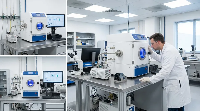
Visual Guide
Related Products
- Molybdenum Tungsten Tantalum Evaporation Boat for High Temperature Applications
- Vacuum Hot Press Furnace Machine for Lamination and Heating
- Aluminized Ceramic Evaporation Boat for Thin Film Deposition
- Tungsten Evaporation Boat for Thin Film Deposition
- Electron Beam Evaporation Coating Oxygen-Free Copper Crucible and Evaporation Boat
People Also Ask
- What is thermal evaporation used to deposit? A Guide to Metals, Compounds, and Key Applications
- What are thermal evaporation sources? Key Types and How to Choose the Right One
- Is thermal evaporation used to deposit a thin metal film? A Guide to This Foundational PVD Technique
- What is the source of evaporation for thin film? Choosing Between Thermal and E-Beam Methods
- What is the difference between thermal evaporation and e beam evaporation? Choose the Right Method for Your Thin Film


