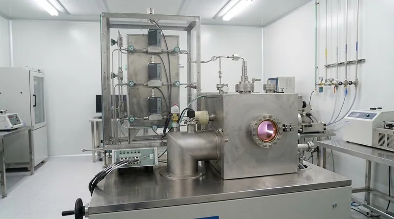
At its core, Chemical Vapor Deposition (CVD) in semiconductor fabrication is a process used to build up the intricate, layered structure of a microchip. It involves introducing specific gases, known as precursors, into a reaction chamber where they chemically react to form a solid thin film on the surface of a silicon wafer. This method is fundamental for creating the insulating and conductive layers that define a modern electronic circuit.
The key to understanding CVD is to see it not as a simple coating technique, but as a precise chemical construction process. It allows engineers to "grow" highly specific materials, atom by atom, onto a substrate, forming the essential electrical pathways and insulators that make a transistor function.
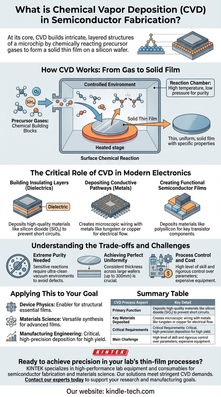
How CVD Works: From Gas to Solid Film
To appreciate why CVD is so vital, you must understand the controlled environment in which it operates. The process is far more sophisticated than simply spraying a material onto a surface.
The Reaction Chamber: A Controlled Environment
A silicon wafer is placed inside a highly controlled reaction chamber. This chamber is typically held at a specific temperature and pressure, often in a vacuum, to ensure process purity and stability. The controlled environment is critical for preventing contamination and enabling the desired chemical reactions.
Precursor Gases: The Chemical Building Blocks
Specific gaseous chemicals, called precursors, are carefully introduced into the chamber. Each precursor contains the atoms needed for the final film. For example, to create a silicon dioxide (SiO₂) insulating layer, precursors like silane (SiH₄) and oxygen (O₂) might be used. The combination and flow rates of these gases are a precise recipe.
The Deposition Process: A Surface Chemical Reaction
The heat and pressure within the chamber energize the precursor gases, causing them to react on the hot surface of the wafer. This chemical reaction breaks the gases down and re-forms them into a new, solid material that deposits evenly across the wafer's surface. The result is a thin, uniform, and solid film with specific electrical or physical properties.
The Critical Role of CVD in Modern Electronics
CVD is not an optional step; it is used repeatedly during chip manufacturing to build circuits layer by layer. Its versatility allows it to deposit the different types of materials required for a functional device.
Building Insulating Layers (Dielectrics)
In a microchip, billions of transistors are packed together. To prevent electrical signals from short-circuiting, they must be separated by insulating materials, or dielectrics. CVD is the primary method for depositing high-quality dielectrics like silicon dioxide and silicon nitride.
Depositing Conductive Pathways (Metals)
CVD is also used to create the microscopic "wiring" that connects transistors. It can deposit metallic films, such as tungsten or copper, that serve as conductive pathways for electricity to flow through the integrated circuit.
Creating Functional Semiconductor Films
Beyond simple insulators and conductors, CVD is used to deposit functional semiconductor materials themselves. For instance, polycrystalline silicon (polysilicon), a key component in a transistor's gate structure, is often deposited using a CVD process.
Understanding the Trade-offs and Challenges
While powerful, CVD is a demanding process with inherent complexities that engineers must manage to ensure high manufacturing yields.
The Need for Extreme Purity
The chemical reactions in CVD are highly sensitive. Any unwanted particles or contaminant gases in the chamber can interfere with the reaction, leading to defects in the film. This is why the process is performed in a vacuum or an ultra-clean environment.
Achieving Perfect Uniformity
For a chip to function correctly, the deposited film must have a consistent thickness across the entire wafer, which can be up to 300mm in diameter. Variations in temperature or gas flow can lead to non-uniformity, causing device performance to vary across the chip.
Process Control and Cost
CVD equipment is highly sophisticated and expensive. The process requires a high level of skill and rigorous control over parameters like temperature, pressure, and gas chemistry to produce reliable and repeatable results.
Applying This to Your Goal
Understanding CVD is essential, but its relevance depends on your specific focus. Use the following to frame its importance for your work.
- If your primary focus is semiconductor device physics: See CVD as the enabler for creating the specific dielectric (insulator) and conductive films that are structurally essential for a transistor to operate as designed.
- If your primary focus is materials science: View CVD as a versatile synthesis technique for creating a wide range of advanced thin films, from standard electronics materials to novel structures like carbon nanotubes and nanowires.
- If your primary focus is manufacturing engineering: Recognize CVD as a critical, high-precision deposition step that demands rigorous process control to ensure consistent film quality, high yield, and cost-effectiveness.
Chemical vapor deposition is a cornerstone of modern technology, enabling the fabrication of the complex micro-devices that power our world.
Summary Table:
| CVD Process Aspect | Key Detail |
|---|---|
| Primary Function | Deposits thin, solid films on silicon wafers via chemical reactions. |
| Key Materials Deposited | Dielectrics (e.g., SiO₂), Conductive Metals (e.g., Tungsten), Semiconductors (e.g., Polysilicon). |
| Critical Requirements | Extreme purity, precise temperature/pressure control, and perfect uniformity. |
| Main Challenge | Sophisticated process control needed to prevent defects and ensure high yield. |
Ready to achieve precision in your lab's thin-film processes? KINTEK specializes in high-performance lab equipment and consumables for semiconductor fabrication and materials science. Whether you are developing next-generation chips or advanced materials, our solutions are designed to meet the stringent demands of CVD and other deposition techniques. Contact our experts today to discuss how we can support your research and manufacturing goals with reliable, cutting-edge technology.
Visual Guide
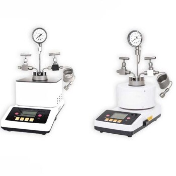
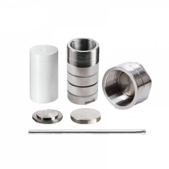
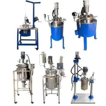
Related Products
- Microwave Plasma Chemical Vapor Deposition MPCVD Machine System Reactor for Lab and Diamond Growth
- 915MHz MPCVD Diamond Machine Microwave Plasma Chemical Vapor Deposition System Reactor
- Customer Made Versatile CVD Tube Furnace Chemical Vapor Deposition Chamber System Equipment
- Cylindrical Resonator MPCVD Machine System Reactor for Microwave Plasma Chemical Vapor Deposition and Lab Diamond Growth
- Split Chamber CVD Tube Furnace with Vacuum Station Chemical Vapor Deposition System Equipment Machine
People Also Ask
- What is microwave plasma chemical vapor deposition? A Guide to High-Purity Diamond Film Growth
- What are the advantages of a Microwave Plasma CVD reactor for MCD/NCD coatings? Precision Multilayer Diamond Engineering
- How do vacuum pumps and valves collaborate in MPCVD? Achieve Precise Pressure Control for Superior CNT Synthesis
- Why is argon-rich gas phase chemistry used for UNCD growth? Unlock Precision Nano-Diamond Synthesis
- How are CVD diamonds created? Discover the Science of Lab-Grown Diamond Precision