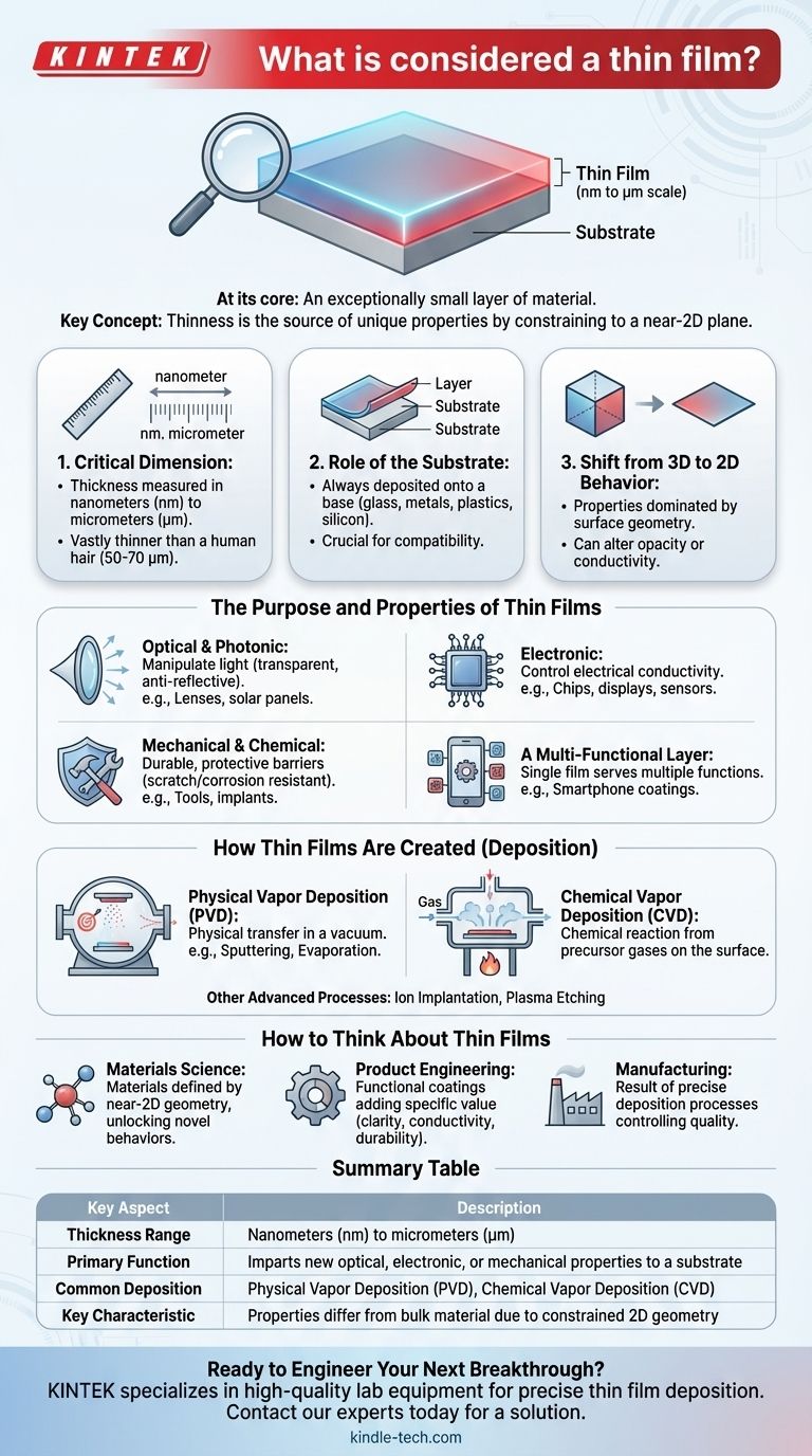
At its core, a thin film is an exceptionally small layer of material. It is deposited onto a surface, known as a substrate, and has a thickness ranging from mere fractions of a nanometer (the scale of a single layer of atoms) up to several micrometers. The defining characteristic is that its thickness is vastly smaller than its length and width, fundamentally altering its physical properties compared to the bulk material.
The critical concept is not just that the film is thin, but that its thinness is the very source of its unique and valuable properties. By constraining the material to a near-two-dimensional plane, we unlock new behaviors in optics, electronics, and mechanics.

Defining Thin Films by More Than Thickness
While the thickness measurement is the most obvious identifier, several other concepts are essential to understanding what constitutes a thin film.
The Critical Dimension: From Nanometers to Micrometers
A thin film's thickness is typically measured in nanometers (nm) or micrometers (µm). For context, a human hair is about 50-70 micrometers thick, meaning most thin films are hundreds or even thousands of times thinner.
This extreme thinness is what suppresses the material's properties in the third dimension, forcing it to behave in ways it otherwise would not.
The Role of the Substrate
Thin films do not exist in isolation. They are always applied or deposited onto a substrate, which is the underlying base material. Common substrates include glass, metals, plastics, and silicon wafers.
The choice of substrate is critical, as it must be compatible with both the deposition process and the final application of the product.
The Shift from 3D to 2D Behavior
Because the film is so thin, it is often described as a two-dimensional material. Its properties are dominated by its surface geometry rather than its volume.
This is the key to why thin films are so useful. A material that is opaque in bulk form might become transparent as a thin film, or an insulator might become a semiconductor.
The Purpose and Properties of Thin Films
Thin films are engineered to impart specific, valuable characteristics to the surface of a substrate. These properties can be grouped into several categories.
Optical and Photonic Properties
Many thin films are designed to manipulate light. They can be made to be highly transparent, anti-reflective, or scratch-resistant, which is essential for applications like eyeglass lenses, camera sensors, and solar panels.
Electronic Properties
Thin films are the bedrock of modern electronics. They can be designed to increase or decrease electrical conductivity, forming the microscopic circuits found in computer chips, displays, and sensors.
Mechanical and Chemical Properties
These films can create a highly durable and protective barrier. They provide scratch resistance, corrosion protection, and a barrier against chemical exposure, extending the life of tools, medical implants, and machine components.
A Multi-Functional Layer
It is common for a single thin film to serve multiple functions. For example, the coating on a smartphone screen is optically transparent, mechanically scratch-resistant, and chemically resistant to oils from your fingers.
A Look at How Thin Films Are Created
The creation of a thin film is a highly controlled engineering process known as deposition. The method used directly influences the film's final properties.
Physical Vapor Deposition (PVD)
PVD involves physically transferring a material onto the substrate in a vacuum. This is often done through sputtering, where ions bombard a target to eject atoms, or evaporation, where a material is heated until it vaporizes and condenses on the substrate.
Chemical Vapor Deposition (CVD)
CVD uses precursor gases that react or decompose on the substrate's surface to form the desired film. Energy, often in the form of heat, is used to initiate the chemical reaction.
Other Advanced Processes
Specialized techniques like ion implantation (directing charged atoms at a surface), plasma etching (using plasma to remove material), and rapid thermal processing (for oxidizing silicon wafers) are also used to create and modify thin films for highly specific applications.
How to Think About Thin Films
Your perspective on thin films will depend on your ultimate goal. Use these points to frame your understanding.
- If your primary focus is materials science: See thin films as materials whose properties are defined by their near-2D geometry, unlocking behaviors not seen in their bulk counterparts.
- If your primary focus is product engineering: View thin films as functional coatings applied to a substrate to add specific value, such as optical clarity, electrical conductivity, or durability.
- If your primary focus is manufacturing: Understand thin films as the result of a precise deposition process (like PVD or CVD) where the technique directly controls the film's quality and characteristics.
Ultimately, these microscopic layers are a foundational technology that enables much of the modern world.
Summary Table:
| Key Aspect | Description |
|---|---|
| Thickness Range | Nanometers (nm) to micrometers (µm) |
| Primary Function | Imparts new optical, electronic, or mechanical properties to a substrate |
| Common Deposition Methods | Physical Vapor Deposition (PVD), Chemical Vapor Deposition (CVD) |
| Key Characteristic | Properties differ from bulk material due to constrained 2D geometry |
Ready to Engineer Your Next Breakthrough with Thin Films?
Thin films are the invisible engine behind advanced electronics, durable coatings, and high-performance optics. Whether you're developing a new semiconductor, a protective coating, or an optical device, the right deposition process is critical to your success.
KINTEK specializes in providing the high-quality lab equipment and consumables needed for precise thin film deposition. From PVD and CVD systems to substrates and targets, we supply the tools that research and production labs rely on.
Let's discuss how we can support your specific application. Contact our experts today to find the perfect solution for your laboratory's thin film needs.
Visual Guide
Related Products
- RF PECVD System Radio Frequency Plasma-Enhanced Chemical Vapor Deposition RF PECVD
- Chemical Vapor Deposition CVD Equipment System Chamber Slide PECVD Tube Furnace with Liquid Gasifier PECVD Machine
- Molybdenum Tungsten Tantalum Evaporation Boat for High Temperature Applications
- Hemispherical Bottom Tungsten Molybdenum Evaporation Boat
- Aluminized Ceramic Evaporation Boat for Thin Film Deposition
People Also Ask
- Why is PECVD environment friendly? Understanding the Eco-Friendly Benefits of Plasma-Enhanced Coating
- What are the advantages of PECVD? Enable Low-Temperature, High-Quality Thin-Film Deposition
- How does RF power create plasma? Achieve Stable, High-Density Plasma for Your Applications
- What are the applications of PECVD? Essential for Semiconductors, MEMS, and Solar Cells
- What is the principle of plasma enhanced chemical vapor deposition? Achieve Low-Temperature Thin Film Deposition