In materials science and engineering, deposition is the highly controlled process of applying a layer of one material onto a surface, known as a substrate. This process builds a thin film—ranging from a single layer of atoms to several micrometers thick—to fundamentally change the substrate's original properties for a specific application.
The core purpose of deposition is not simply to coat a surface. It is a precision engineering technique used to fundamentally redesign a material's characteristics—such as its electrical conductivity, hardness, or optical behavior—by building a new, functional layer from the atom up.
The Core Principle: Modifying a Surface, Atom by Atom
Deposition is a foundational process in fields like semiconductor manufacturing, optics, and advanced materials. It operates on a simple but powerful principle: a base material can be given entirely new capabilities by adding a precisely constructed surface layer.
What is the Substrate?
The substrate is the base material or workpiece that receives the coating. Think of it as the canvas on which the new layer is built.
A substrate can be anything from a silicon wafer for a computer chip to a piece of glass for an optical lens or a metal tool bit that needs a hardened surface.
What is the Deposited Film?
The thin film is the new layer of material that is synthesized or grown on the substrate's surface. This process happens atom-by-atom or molecule-by-molecule.
The thickness of this film is critical and is controlled with incredible precision, often measured in nanometers (billionths of a meter).
The Goal: Engineering New Properties
The primary goal is to combine the desirable properties of the substrate (like its cost or structural integrity) with the properties of the deposited film (like its conductivity or hardness).
For example, a non-conductive piece of plastic can be made conductive for an electronic device, or a standard piece of steel can be given a diamond-like carbon coating to make it extremely wear-resistant.
The Critical Role of Preparation and Environment
Successful deposition is impossible without an impeccably prepared substrate and a strictly controlled environment. The quality of the final film is determined long before the deposition process even begins.
Meticulous Cleaning
The substrate must be perfectly clean. Contaminants like dust or oils, even on a microscopic scale, will prevent the deposited film from adhering correctly and will create defects.
This is why processes like ultrasonic cleaning are a standard and non-negotiable first step.
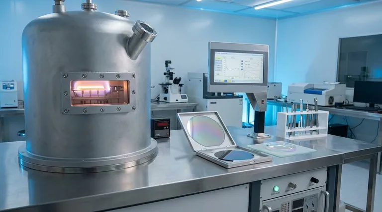
The Necessity of a Vacuum
Most high-precision deposition occurs in a vacuum chamber. The substrate is often moved from a preparation area (a "load lock") into the main chamber without breaking this vacuum.
The vacuum is essential to remove air and other molecules that could otherwise react with and contaminate the film as it forms, ensuring the layer is made of only the intended material.
Preparing the Surface for Adhesion
To ensure the new atoms stick properly, the substrate is often preheated using electron beams or infrared lamps.
This heating process gives the arriving atoms enough energy to find the optimal position on the surface, which promotes strong adhesion and the formation of a smooth, uniform film.
Common Pitfalls to Avoid
While powerful, deposition is a sensitive process where small errors can lead to complete failure. Understanding these challenges is key to achieving a successful outcome.
Contamination is the Enemy
The single greatest cause of failure is contamination. Impurities from the substrate, the deposition chamber, or the material source itself can ruin the film's intended electrical, optical, or mechanical properties.
Adhesion Isn't Guaranteed
A film is useless if it peels or flakes off. Poor adhesion can result from improper substrate cleaning, a chemical incompatibility between the film and substrate, or internal stresses that build up in the film during growth.
Uniformity Requires Precision
Achieving a perfectly even film thickness across the entire surface of the substrate is a significant technical challenge. It requires sophisticated equipment and exact control over all process variables, from temperature to pressure.
Making the Right Choice for Your Goal
The specific goal of your project dictates how and why you use deposition.
- If your primary focus is creating a protective barrier: Deposition is the ideal method for adding a hard, corrosion-resistant, or scratch-resistant layer onto a less durable base material.
- If your primary focus is altering optical properties: Thin films are essential for creating the anti-reflective coatings on eyeglasses, specialized filters for cameras, and coatings on architectural glass.
- If your primary focus is fabricating electronics: The entire semiconductor industry is built on the precise deposition of multiple layers of conductive, insulating, and semi-conductive materials onto silicon substrates.
Ultimately, mastering deposition is about controlling matter at the atomic scale to engineer the surfaces that define modern technology.
Summary Table:
| Aspect | Key Takeaway |
|---|---|
| Core Principle | Atom-by-atom addition of a material layer to a substrate to engineer new properties. |
| Critical Factor | Requires a meticulously clean substrate and a controlled vacuum environment to prevent contamination. |
| Primary Goal | To combine the bulk properties of a substrate with the surface properties of a thin film (e.g., conductivity, hardness). |
| Common Applications | Semiconductor manufacturing, optical coatings, wear-resistant surfaces, and advanced electronics. |
Ready to Engineer Your Material's Surface?
Mastering deposition requires precision equipment and expertise. KINTEK specializes in high-performance lab equipment and consumables for all your thin-film deposition needs. Whether you are developing semiconductors, optical coatings, or protective layers, our solutions ensure the clean, controlled environments necessary for success.
Contact KINTEK today to discuss how we can support your laboratory's specific deposition challenges and help you achieve flawless results.
Visual Guide

Related Products
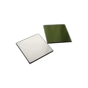
- Optical Window Glass Substrate Wafer Quartz Plate JGS1 JGS2 JGS3
- RF PECVD System Radio Frequency Plasma-Enhanced Chemical Vapor Deposition RF PECVD
- Evaporation Boat for Organic Matter
- Chemical Vapor Deposition CVD Equipment System Chamber Slide PECVD Tube Furnace with Liquid Gasifier PECVD Machine
- Custom CVD Diamond Coating for Lab Applications
People Also Ask
- What is the maximum temperature for quartz windows? Ensure Long-Term Reliability and Avoid Devitrification
- Can quartz glass be heated? Mastering High-Temperature Applications with Quartz
- How does quartz differ from glass? A Guide to Material Selection for Performance
- What is the working temperature of quartz glass? Master Its High-Temp Limits & Applications
- What is the temperature range of quartz glass? Master Its Thermal Limits for Demanding Applications