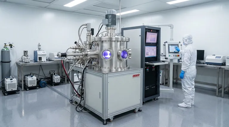
At its core, a magnetron sputtering machine is a highly precise piece of equipment that deposits an ultra-thin layer of one material onto the surface of another inside a vacuum. It works by creating an energized gas (plasma) and using a magnetic field to bombard a source material (the "target"), which ejects atoms that then coat a desired object (the "substrate"). This process allows for the creation of high-performance functional films.
A magnetron sputtering system is not simply a coating machine; it is a sophisticated tool for engineering surfaces at the atomic level. It leverages plasma physics and magnetism within a vacuum to build high-purity, high-performance thin films that are impossible to create through conventional means.
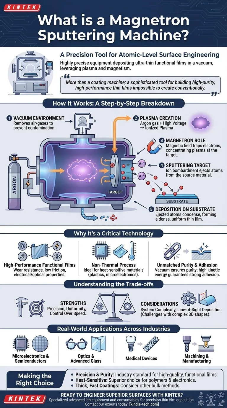
How Magnetron Sputtering Works: A Step-by-Step Breakdown
To understand the machine, you must first understand the process. Each step is carefully controlled to achieve a specific outcome on the material's surface.
The Vacuum Environment
First, the entire process occurs within a vacuum chamber. Removing air and other gases is critical to prevent contamination and ensure the sputtered atoms can travel freely from the target to the substrate.
Creating the Plasma
An inert gas, typically Argon, is introduced into the chamber. A high-voltage power supply then energizes the gas, stripping electrons from the Argon atoms and creating a glowing, ionized gas known as plasma.
The Role of the Magnetron
This is the key to the technology. A powerful magnetron is placed behind the target material. Its magnetic field traps the free electrons from the plasma near the surface of the target.
These trapped electrons collide with more Argon atoms, dramatically increasing the efficiency of the ionization process. This creates a dense, concentrated plasma directly in front of the target.
Sputtering the Target
The positively charged Argon ions in the dense plasma are accelerated by the electric field and slam into the negatively charged target material with immense force.
This physical bombardment, known as sputtering, has enough energy to knock individual atoms or molecules off the target material, ejecting them into the vacuum chamber.
Deposition onto the Substrate
The ejected atoms from the target travel through the vacuum and land on the substrate—the object being coated.
As these atoms accumulate, they condense and build up, layer by layer, to form a very thin, highly uniform, and dense film.
Why Magnetron Sputtering is a Critical Technology
The value of this technology lies not just in coating an object, but in the specific properties of the films it creates. It solves problems that other coating methods cannot.
Creating High-Performance Functional Films
Sputtering allows for the deposition of films with highly specific and engineered properties, such as wear resistance, low friction, corrosion resistance, or particular electrical and optical characteristics.
A Non-Thermal Process
The deposition occurs without generating significant heat. This makes it the ideal technology for coating heat-sensitive materials, such as plastics and complex microelectronics, which would be damaged by other high-temperature methods.
Unmatched Purity and Adhesion
The vacuum environment prevents impurities, and the high kinetic energy of the sputtered atoms ensures the resulting film is dense and adheres strongly to the substrate surface. This is critical for durable medical implants and reliable electronic components.
Understanding the Trade-offs
While powerful, magnetron sputtering is a specialized tool. Understanding its strengths and limitations is key to using it effectively.
Strength: Precision Over Speed
Magnetron sputtering offers unparalleled control over film thickness, uniformity, and composition. This precision can mean the deposition rates are slower than bulk coating methods like electroplating or thermal evaporation.
Consideration: System Complexity
A magnetron sputtering system is sophisticated equipment. It requires a high-vacuum chamber, specialized power supplies, and magnetic assemblies, making it more complex and costly than simpler coating techniques.
Consideration: Line-of-Sight Deposition
The sputtered atoms travel in a relatively straight line. This means the process is best suited for coating flat or gently curved surfaces, as it can be challenging to uniformly coat complex, three-dimensional shapes with deep recesses.
Real-World Applications Across Industries
The unique capabilities of magnetron sputtering have made it indispensable in numerous high-tech fields.
Microelectronics and Semiconductors
It is a cornerstone of the semiconductor industry for producing the intricate layers in integrated circuits, gate dielectrics, and sensors. It was also a foundational technology for manufacturing computer hard disks.
Optics and Advanced Glass
The technology is used to deposit anti-reflective coatings on lenses and to create low-emissivity (Low-E) films on architectural glass, which reflect thermal radiation and improve energy efficiency.
Medical Devices
In the medical field, it is used to create biocompatible and anti-rejection coatings on dental and surgical implants, as well as highly durable coatings on angioplasty devices and other critical components.
Machining and Manufacturing
Sputtering is used to apply super-hard and self-lubricating films onto cutting tools and mechanical parts, dramatically increasing their lifespan and performance.
Making the Right Choice for Your Goal
Deciding whether to use magnetron sputtering depends entirely on your end goal for the surface you are creating.
- If your primary focus is creating high-purity, functional films with specific optical or electrical properties: Magnetron sputtering is the industry standard for precision and control.
- If you are working with heat-sensitive substrates like polymers or finished electronic assemblies: The non-thermal nature of the process makes it a superior and often necessary choice.
- If your goal is simply to apply a thick, protective coating at the lowest cost and highest speed: You may want to evaluate other bulk deposition methods.
Ultimately, magnetron sputtering empowers us to engineer the surfaces of materials, unlocking performance and functionality that drive modern technology forward.
Summary Table:
| Key Aspect | Description |
|---|---|
| Process | Vacuum-based thin-film deposition using plasma and magnetic fields |
| Key Benefit | Creates high-purity, functional films with precise control |
| Ideal For | Heat-sensitive substrates, microelectronics, medical implants, optical coatings |
| Main Limitation | Line-of-sight deposition; complex 3D shapes can be challenging |
| Common Applications | Semiconductor manufacturing, medical devices, architectural glass, cutting tools |
Ready to Engineer Superior Surfaces with Magnetron Sputtering?
KINTEK specializes in advanced lab equipment and consumables for precision thin-film deposition. Whether you're developing semiconductors, medical implants, or optical coatings, our magnetron sputtering solutions deliver the unmatched purity, adhesion, and control your R&D or production requires.
Contact our experts today to discuss how we can help you achieve your specific coating goals and enhance your material performance.
Visual Guide
Related Products
- Three-dimensional electromagnetic sieving instrument
- Metallographic Specimen Mounting Machine for Laboratory Materials and Analysis
People Also Ask
- What are the limitations of sieving? Understanding the Constraints of Particle Size Analysis
- What are the precautions for sieving method? Ensure Accurate Particle Size Analysis
- What is the advantage of sieving? A Simple, Reliable Method for Particle Size Analysis
- What mixtures can be separated by sieving? A Guide to Efficient Solid-Solid Separation
- Why is sieving equipment essential for the classification of processed bio-activated carbon? Optimize Performance