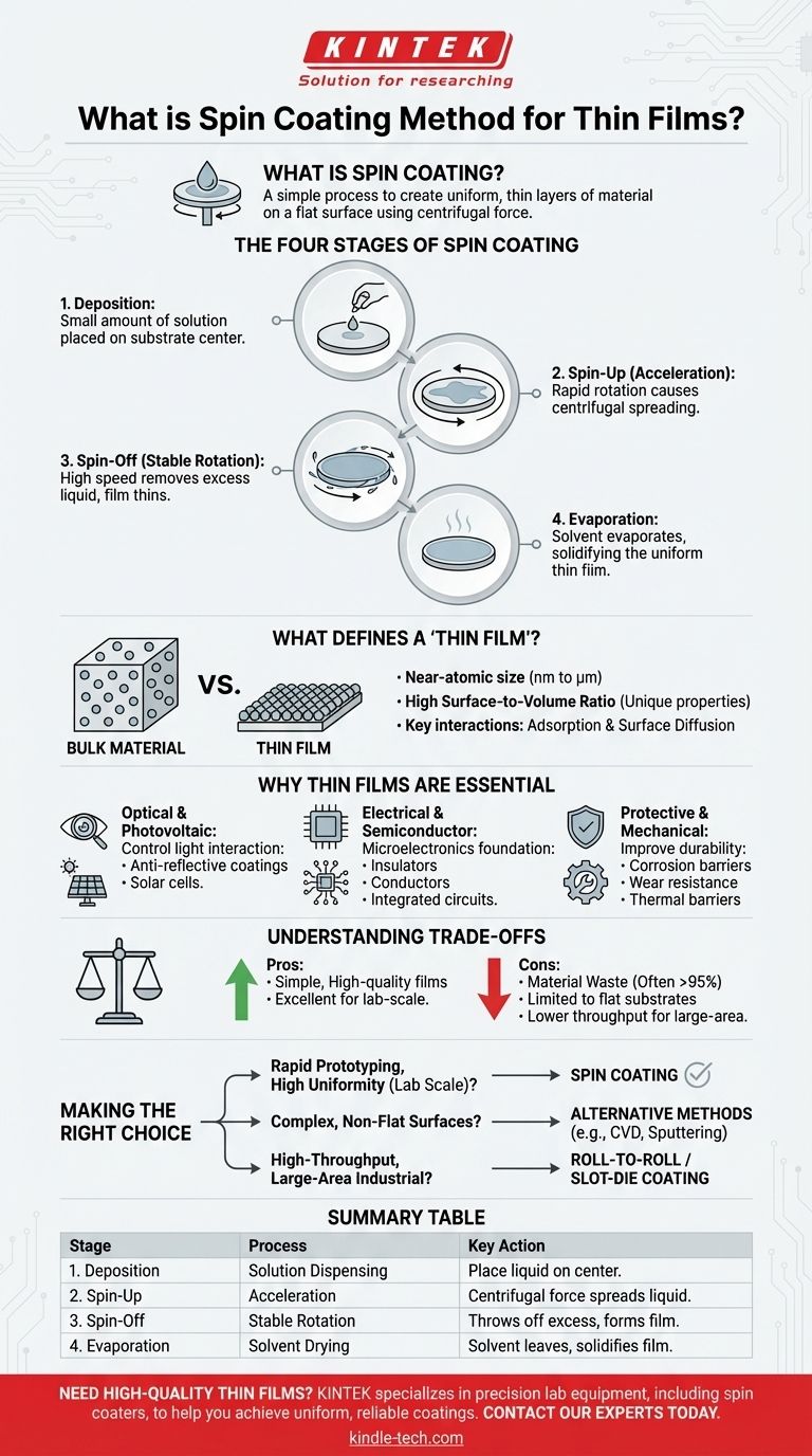
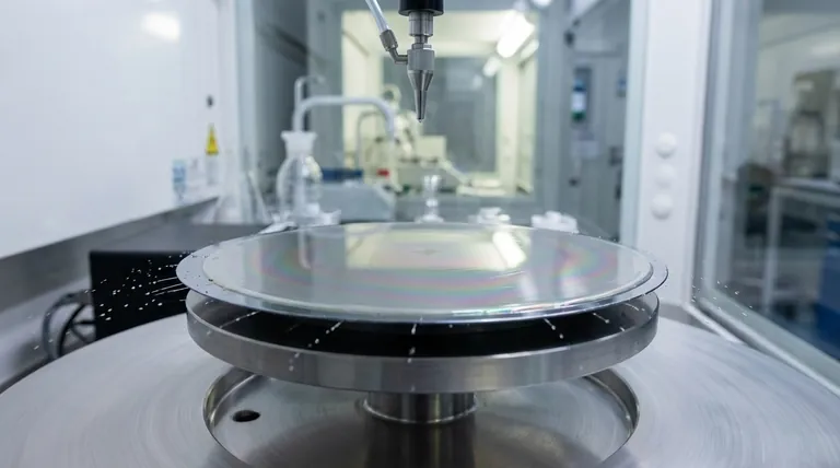
In essence, spin coating is a straightforward process used to create uniform, thin layers of material on a flat surface. A small amount of a liquid solution is placed on the center of a substrate, which is then spun at high speed, causing centrifugal force to spread the liquid into a thin, even film.
The core principle of spin coating is using controlled centrifugal force to overcome surface tension, spreading a liquid material into a microscopically thin, uniform layer as the solvent evaporates. This simple, rapid technique is fundamental to manufacturing many high-technology components, from microchips to optical lenses.
The Mechanics of the Spin Coating Process
Spin coating is valued for its simplicity and the high quality of the films it produces. The entire process can be broken down into a few distinct stages that happen in rapid succession.
Stage 1: Deposition
A small excess of the coating solution is dispensed onto the center of the substrate. The volume is just enough to cover the entire surface once spread.
Stage 2: Spin-Up (Acceleration)
The substrate is rapidly accelerated to its final, desired rotation speed. The liquid flows radially outward due to centrifugal force, beginning the spreading process.
Stage 3: Spin-Off (Stable Rotation)
The substrate spins at a constant, high speed. Excess solution is thrown off the edge of the substrate, and the remaining liquid thins out into a film. Viscous forces and centrifugal force dominate this stage.
Stage 4: Evaporation
As the film continues to thin, solvent evaporation becomes the dominant factor in finalizing the film's thickness. The film solidifies as the solvent leaves, resulting in a stable, solid thin layer.
What Defines a "Thin Film"?
To understand the purpose of spin coating, you must first understand the unique nature of thin films. They are not simply smaller versions of bulk materials; their properties are fundamentally different.
From Bulk Material to Atomic Scale
A thin film is a layer of material ranging from a few nanometers to several micrometers in thickness. By reducing a material to this near-atomic size, its physical and chemical behaviors change dramatically.
The Surface-to-Volume Ratio Advantage
In bulk materials, most atoms are surrounded by other atoms. In a thin film, a much higher proportion of atoms are at a surface. This high surface-to-volume ratio is what gives thin films their unique optical, electrical, and mechanical properties.
Key Material Interactions
The formation and stability of these films rely on atomic-level processes. Adsorption is the process of atoms from the liquid solution attaching to the substrate surface, while surface diffusion allows these atoms to move and arrange themselves into an orderly film.
Why Thin Films are Essential in Modern Technology
The unique properties of thin films make them indispensable across a vast range of industries, from consumer electronics to aerospace engineering.
Optical and Photovoltaic Applications
Thin films are used to control the way light interacts with a surface. This includes the anti-reflective coatings on eyeglasses, the reflective metal layer on the back of a mirror, and the critical layers in solar cells that convert light into electricity.
Electrical and Semiconductor Applications
The entire microelectronics industry is built on thin films. They are used to create the intricate patterns of insulators, conductors, and semiconductors that form integrated circuits, microprocessors, and touch-panel displays.
Protective and Mechanical Applications
Thin films can dramatically improve the durability of a substrate. They create protective barriers against corrosion, provide wear resistance on cutting tools, and act as thermal barriers in high-temperature environments like jet engines.
Understanding the Trade-offs of Spin Coating
While effective, spin coating is not a universal solution. Understanding its limitations is key to using it appropriately.
Material Waste
A significant portion of the initial coating solution—often over 95%—is spun off the edge of the substrate and wasted. This can be costly when using expensive materials.
Substrate Shape Limitations
The process works almost exclusively for flat, planar substrates. It is not suitable for coating complex, three-dimensional, or non-circular objects.
Area and Throughput
Spin coating is excellent for laboratory-scale work and coating individual wafers or substrates. However, it can be inefficient for very large-area industrial applications, where other methods like roll-to-roll coating may be preferred.
Making the Right Choice for Your Application
Selecting the right deposition method depends entirely on your project's goals, materials, and scale.
- If your primary focus is rapid prototyping and high uniformity on a lab scale: Spin coating is an excellent, cost-effective, and reliable choice for flat substrates.
- If your primary focus is coating complex, non-flat surfaces: You will need to explore alternative deposition techniques like chemical vapor deposition (CVD) or sputtering.
- If your primary focus is high-throughput, large-area industrial production: Consider methods like slot-die coating or roll-to-roll processing to minimize material waste and maximize efficiency.
Ultimately, mastering thin film technology begins with matching the simplicity of a method like spin coating to the complexity of the desired outcome.
Summary Table:
| Stage | Process | Key Action |
|---|---|---|
| 1. Deposition | Solution Dispensing | Liquid coating material is placed on the substrate center. |
| 2. Spin-Up | Acceleration | Substrate rapidly spins up, centrifugal force spreads the liquid. |
| 3. Spin-Off | Stable Rotation | High-speed rotation throws off excess liquid, forming a thin film. |
| 4. Evaporation | Solvent Drying | Solvent evaporates, leaving a solid, uniform thin film on the substrate. |
Need high-quality thin films for your research or production? KINTEK specializes in precision lab equipment, including spin coaters and consumables, to help you achieve uniform, reliable coatings for your microelectronics, optics, or semiconductor projects. Contact our experts today to discuss your specific application and find the perfect solution for your laboratory needs!
Visual Guide