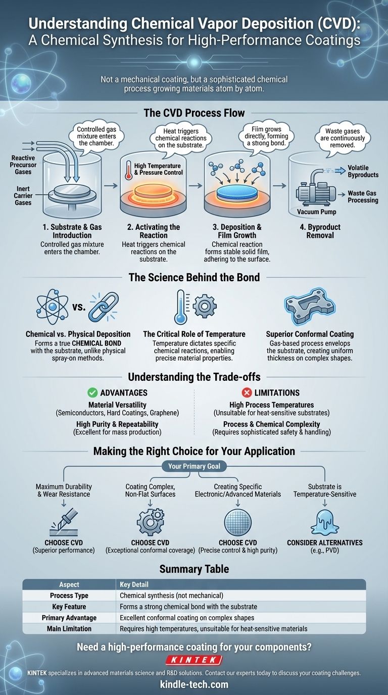
At its core, Chemical Vapor Deposition (CVD) is a sophisticated process for creating high-performance, solid thin films on a surface. It achieves this not by spraying a material, but by introducing volatile precursor gases into a chamber, which then react and decompose on a heated substrate to "grow" a new material layer directly onto it, atom by atom.
The crucial insight is that CVD is fundamentally a chemical synthesis process, not a mechanical coating method. This creates a powerful chemical bond between the film and the substrate, resulting in exceptionally durable and highly pure materials that are grown, not just applied.
Deconstructing the CVD Process
The CVD technique follows a precise sequence of steps within a controlled reaction chamber to ensure a uniform and high-quality film is created.
Step 1: Substrate and Gas Introduction
A substrate, which is the object to be coated, is placed inside the reaction chamber. A carefully managed mixture of reactive precursor gases and inert carrier gases is then introduced into the chamber.
Step 2: Activating the Reaction
The substrate is heated to a specific, often high, temperature. This heat provides the necessary energy to trigger the chemical reactions. The pressure within the chamber is also precisely controlled to influence the reaction rate and film characteristics.
Step 3: Deposition and Film Growth
As the precursor gases come into contact with the hot substrate, they decompose or react. This chemical reaction forms a stable, solid film that deposits and adheres to the substrate's surface. In many cases, the substrate itself acts as a catalyst, promoting the reaction and ensuring a strong bond.
Step 4: Byproduct Removal
The chemical reactions create volatile byproducts. These waste gases are continuously pumped out of the chamber and properly processed to prevent environmental contamination.
The Science Behind the Bond
The unique properties of CVD coatings stem from the nature of the deposition process itself. It’s a bottom-up approach to material creation.
Chemical vs. Physical Deposition
Unlike Physical Vapor Deposition (PVD), which is more akin to atomic-level spray painting, CVD forms a true chemical bond with the substrate. This integration of the coating into the surface makes CVD films exceptionally adherent and often more resistant to abrasion and wear.
The Critical Role of Temperature
Temperature is the primary lever in the CVD process. It dictates the specific chemical reaction that will occur on the substrate's surface. By controlling the temperature and the composition of the precursor gases, engineers can deposit a wide variety of materials with distinct properties.
Superior Conformal Coating
Because the deposition relies on a gas that envelops the entire substrate, CVD excels at creating a conformal coating. This means the film grows with uniform thickness over complex, irregular, and three-dimensional shapes, a significant advantage for components like drill bits or intricate electronic parts.
Understanding the Trade-offs
While powerful, CVD is not the universal solution for every application. Understanding its advantages and limitations is key to using it effectively.
Advantage: Material Versatility
CVD is incredibly versatile. It can be used to deposit a vast range of materials, including:
- Dielectric films like Silicon Dioxide (SiO₂) and Silicon Nitride (Si₃N₄) for semiconductors.
- Hard materials for wear-resistant tool coatings.
- Highly pure semiconductor films.
- Advanced materials like graphene, grown on a metal catalyst surface.
Advantage: High Purity and Repeatability
The controlled nature of the process allows for the creation of films with very high purity and structural quality. Once a process is dialed in, it offers excellent repeatability for mass production.
Limitation: High Process Temperatures
The need for high substrate temperatures is a major constraint. These temperatures can damage or fundamentally alter heat-sensitive substrates, making CVD unsuitable for many plastics, low-melting-point metals, or pre-processed electronic components.
Limitation: Process and Chemical Complexity
CVD involves handling volatile, and sometimes toxic or corrosive, precursor gases and byproducts. This requires sophisticated safety and handling equipment, adding to the overall cost and complexity of the operation compared to simpler coating methods.
Making the Right Choice for Your Application
Selecting the right coating technology depends entirely on your end goal and substrate limitations.
- If your primary focus is maximum durability and wear resistance: CVD is an excellent choice for applications like cutting tools, where its chemically bonded, hard coating provides superior performance.
- If your primary focus is coating complex, non-flat surfaces: CVD's gas-based nature provides exceptional conformal coverage that is difficult to achieve with line-of-sight methods.
- If your primary focus is creating specific electronic or advanced materials: CVD offers the precise control needed to grow high-purity films like semiconductors or graphene with specific properties.
- If your substrate is temperature-sensitive: You must carefully evaluate if the material can withstand the high process temperatures; if not, an alternative like PVD is the necessary choice.
Ultimately, choosing CVD is a decision to build a material directly onto your component, offering unparalleled control and performance for the most demanding applications.
Summary Table:
| Aspect | Key Detail |
|---|---|
| Process Type | Chemical synthesis (not mechanical) |
| Key Feature | Forms a strong chemical bond with the substrate |
| Primary Advantage | Excellent conformal coating on complex shapes |
| Main Limitation | Requires high temperatures, unsuitable for heat-sensitive materials |
Need a high-performance coating for your components?
KINTEK specializes in advanced lab equipment and consumables for materials science and R&D. Whether you are developing semiconductor devices, wear-resistant tools, or advanced materials like graphene, our expertise can help you select the right CVD solution for your specific substrate and performance requirements.
Contact our experts today to discuss how we can support your laboratory's coating and material synthesis challenges.
Visual Guide
Related Products
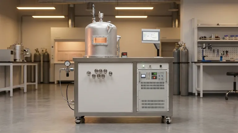
- HFCVD Machine System Equipment for Drawing Die Nano-Diamond Coating
- Custom CVD Diamond Coating for Lab Applications
- Chemical Vapor Deposition CVD Equipment System Chamber Slide PECVD Tube Furnace with Liquid Gasifier PECVD Machine
- Customer Made Versatile CVD Tube Furnace Chemical Vapor Deposition Chamber System Equipment
- RF PECVD System Radio Frequency Plasma-Enhanced Chemical Vapor Deposition RF PECVD
People Also Ask
- Why is Chemical Vapor Deposition (CVD) equipment uniquely suited for constructing hierarchical superhydrophobic structures?
- How expensive is chemical vapor deposition? Understanding the True Cost of High-Performance Coating
- What is the chemical vapor deposition growth process? Build Superior Thin Films from the Atom Up
- What is the full form of HFCVD? A Guide to Hot Filament Chemical Vapor Deposition
- What are the disadvantages and challenges of the HFCVD method? Overcome Growth Limits and Filament Issues


