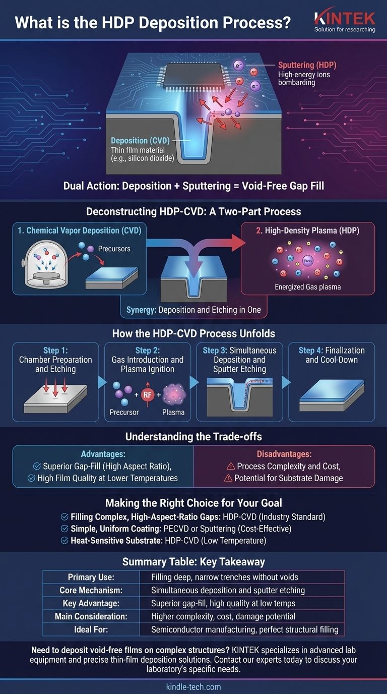
In essence, High-Density Plasma Chemical Vapor Deposition (HDP-CVD) is an advanced manufacturing process used to deposit high-quality thin films, particularly for filling microscopic gaps in complex structures like microchips. It enhances standard Chemical Vapor Deposition (CVD) by using an energized, high-density plasma that simultaneously deposits material and etches it away, resulting in exceptionally uniform and void-free layers.
While standard deposition techniques simply coat a surface, HDP-CVD uniquely combines the act of adding material (deposition) with the act of selectively removing it (sputtering). This dual action is the key to its ability to fill deep, narrow trenches without leaving voids or seams.
Deconstructing HDP-CVD: A Two-Part Process
To understand HDP-CVD, you must first understand its constituent parts: the deposition method (CVD) and the enhancement that makes it unique (the High-Density Plasma).
The Foundation: Chemical Vapor Deposition (CVD)
At its core, HDP-CVD is a type of chemical vapor deposition. The fundamental principle of CVD involves placing a component, or substrate, inside a vacuum chamber.
Specific gaseous chemicals, known as precursors, are then introduced into the chamber. These gases react on the heated surface of the substrate, creating a solid thin film of the desired material.
The process involves several distinct steps, from the transport of gases to the surface, their chemical reaction, and finally the growth of the film on the substrate.
The Enhancement: High-Density Plasma (HDP)
The "HDP" part is what makes this process so powerful. A plasma is a state of matter where a gas is energized until its atoms are ionized, creating a mix of ions and electrons.
In HDP-CVD, a very high-density plasma is generated, meaning it contains a significantly higher concentration of ions than in standard plasma-based deposition methods. This dense cloud of high-energy ions fundamentally changes the deposition dynamics.
The Synergy: Deposition and Etching in One
Herein lies the critical difference. In HDP-CVD, two processes happen at the same time:
- Deposition: The precursor gases react to form a film on the substrate, just like in standard CVD.
- Sputtering: The high-energy ions from the plasma bombard the substrate, physically knocking off or "sputtering" away some of the freshly deposited material.
This simultaneous sputtering is not random. It preferentially etches the corners and overhangs of features, allowing the deposition material to fill deep trenches from the bottom up, preventing the formation of voids.
How the HDP-CVD Process Unfolds
A typical HDP-CVD process follows a precise sequence to achieve its unique gap-filling capability.
Step 1: Chamber Preparation and Etching
The substrate is placed in the vacuum chamber, which is pumped down to a very low pressure. The substrate may be heated to the target process temperature.
Often, a preliminary etching step is performed using ions to clean the substrate surface of any contaminants, ensuring the film adheres perfectly.
Step 2: Gas Introduction and Plasma Ignition
The precursor gases and an inert gas (like Argon) are introduced into the chamber. Radio frequency (RF) energy is then applied to ignite the gases into a high-density plasma.
Step 3: Simultaneous Deposition and Sputter Etching
As the precursor gases deposit material onto the surface, the high-energy ions from the plasma bombard the film.
This bombardment has a higher impact on angled surfaces, effectively sputtering away material that builds up at the top corners of a trench. This keeps the trench open, allowing deposition material to continue filling the bottom.
Step 4: Finalization and Cool-Down
Once the desired film thickness is achieved, the gases and RF power are turned off. The chamber is returned to ambient pressure and the finished substrate is removed.
Understanding the Trade-offs
HDP-CVD is a specialized tool, not a universal solution. Understanding its pros and cons is essential for proper application.
Advantage: Superior Gap-Fill
This is the primary reason for using HDP-CVD. Its ability to fill high-aspect-ratio (deep and narrow) trenches and gaps without creating voids is unmatched by most other deposition techniques.
Advantage: High Film Quality at Lower Temperatures
The energy supplied by the plasma allows for the formation of dense, high-quality films at much lower substrate temperatures compared to purely thermal CVD processes. This makes it suitable for substrates that cannot withstand high heat.
Disadvantage: Process Complexity and Cost
The equipment required for HDP-CVD is sophisticated and expensive. Maintaining the delicate balance between the deposition rate and the sputter-etch rate requires precise control and expertise.
Disadvantage: Potential for Substrate Damage
The same high-energy ion bombardment that enables gap-fill can also cause physical damage to the underlying substrate if the process is not perfectly optimized.
Making the Right Choice for Your Goal
Selecting a deposition method depends entirely on the film's intended function and the geometry of the substrate.
- If your primary focus is filling complex, high-aspect-ratio gaps: HDP-CVD is the industry-standard solution for this exact challenge, especially in semiconductor manufacturing.
- If your primary focus is a simple, uniform coating on a flat surface: A less complex method like standard Plasma-Enhanced CVD (PECVD) or Sputtering (a PVD technique) is likely more efficient and cost-effective.
- If your primary focus is depositing on a heat-sensitive substrate: HDP-CVD is an excellent choice due to its ability to produce high-quality films at relatively low temperatures.
Ultimately, choosing HDP-CVD is a decision to prioritize perfect, void-free structural filling over process simplicity and cost.
Summary Table:
| Aspect | Key Takeaway |
|---|---|
| Primary Use | Filling deep, narrow trenches and gaps (e.g., in microchips) without voids. |
| Core Mechanism | Simultaneous deposition of material and sputter etching by a high-density plasma. |
| Key Advantage | Superior gap-fill capability and high-quality films at lower temperatures. |
| Main Consideration | Higher process complexity, cost, and potential for substrate damage. |
| Ideal For | Semiconductor manufacturing and applications requiring perfect structural filling. |
Need to deposit void-free films on complex structures?
KINTEK specializes in advanced lab equipment, including solutions for precise thin-film deposition. Our expertise can help you select the right technology to enhance your research and development, ensuring high-quality results for your most challenging substrates.
Contact our experts today to discuss how we can support your laboratory's specific needs.
Visual Guide
Related Products
- HFCVD Machine System Equipment for Drawing Die Nano-Diamond Coating
- Microwave Plasma Chemical Vapor Deposition MPCVD Machine System Reactor for Lab and Diamond Growth
- 915MHz MPCVD Diamond Machine Microwave Plasma Chemical Vapor Deposition System Reactor
- Inclined Rotary Plasma Enhanced Chemical Vapor Deposition PECVD Equipment Tube Furnace Machine
- Chemical Vapor Deposition CVD Equipment System Chamber Slide PECVD Tube Furnace with Liquid Gasifier PECVD Machine
People Also Ask
- What are the advantages of chemical vapor deposition? Achieve Superior Thin Films for Your Lab
- What is the specific function of the metal filament in HF-CVD? Key Roles in Diamond Growth
- What is the function of tungsten filaments in HFCVD? Powering Diamond Film Synthesis with Thermal Excitation
- What is the hot filament chemical vapour deposition of diamond? A Guide to Synthetic Diamond Coating
- How expensive is chemical vapor deposition? Understanding the True Cost of High-Performance Coating


