In essence, Physical Vapor Deposition (PVD) is a vacuum-based process used to create nanoparticles and thin films. It works by physically transforming a solid source material into a vapor through methods like intense heating or ion bombardment. This vapor then travels through the vacuum and condenses on a surface or within an inert gas to form extremely pure, high-quality nanoparticles.
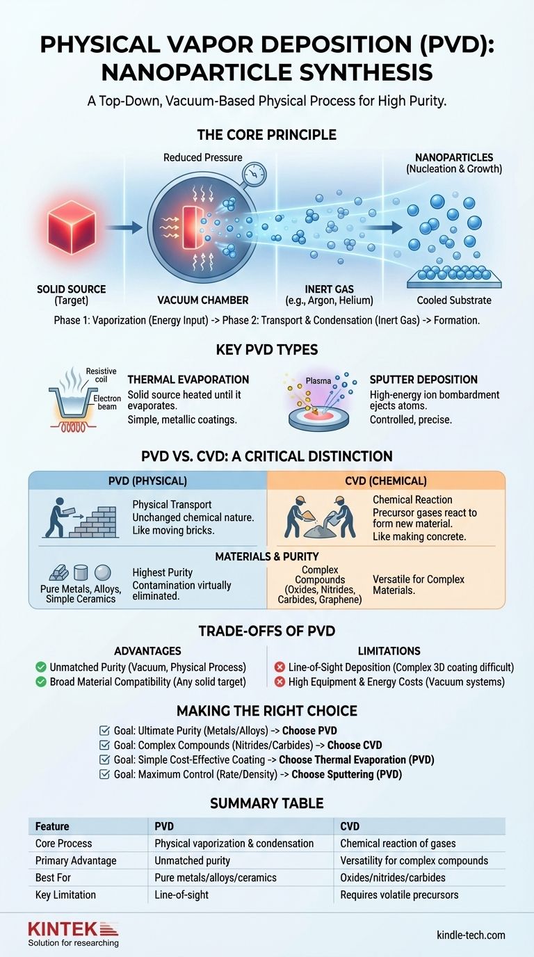
Physical Vapor Deposition (PVD) is a "top-down" synthesis method that creates nanoparticles through purely physical means—vaporization and condensation—in a vacuum. This distinguishes it from chemical methods and makes it ideal for producing materials of the highest purity.
The Core Principle: From Solid to Vapor to Nanoparticle
To understand PVD, it's best to think of it as a three-phase process that happens inside a highly controlled vacuum chamber. This process is fundamentally physical, meaning no chemical reactions are intended to occur.
The Vacuum Environment
First, the entire process takes place in a high-vacuum chamber. This is critical because it removes atmospheric gases that could otherwise react with the vapor and contaminate the final nanoparticles. A vacuum also allows the vaporized atoms to travel in a straight line from the source to their destination.
Phase 1: Vaporization
The goal of this phase is to turn a solid material (known as the "target" or "source") into a gas. This is achieved through immense energy input, primarily using one of two methods. We will explore these methods in detail shortly.
Phase 2: Transport and Condensation
Once atoms are liberated from the solid source, they travel through the vacuum chamber. To form nanoparticles, this vapor is often directed into a stream of cool, inert gas (like Argon or Helium). The vapor rapidly cools, causing the atoms to collide and stick together, a process called nucleation and growth, which forms the nanoparticles.
Key Types of Physical Vapor Deposition
While the principle is the same, the method of vaporization defines the specific type of PVD. The two most common techniques are Thermal Evaporation and Sputtering.
Thermal Evaporation
This is the conceptually simplest form of PVD. The source material is placed in a crucible and heated by a resistive element or an electron beam until it literally boils and evaporates. This metallic vapor then travels through the chamber to condense.
Sputter Deposition (Sputtering)
Sputtering is a more energetic and controlled process. Instead of heat, it uses a high-energy plasma of an inert gas (like Argon). Positively charged Argon ions are accelerated into the negatively charged source target, bombarding it like microscopic sandblasting. This bombardment has enough force to physically knock atoms off the target, ejecting them into the vacuum.
PVD vs. CVD: A Critical Distinction
It is easy to confuse Physical Vapor Deposition (PVD) with Chemical Vapor Deposition (CVD), but they operate on fundamentally different principles.
The "How": Physical vs. Chemical
PVD is a physical process. It moves atoms from a solid source to a substrate or condensation zone without changing their chemical nature. Think of it as physically transporting bricks from one place to another.
CVD is a chemical process. It introduces one or more volatile precursor gases into a chamber, which then react and decompose on a heated surface to form the desired material. This is like bringing sand and cement to a location and then mixing them to create concrete.
The Materials
PVD excels at depositing pure metals, alloys, and certain ceramic compounds. Because it starts with a solid, high-purity source, the final nanoparticles or film are also exceptionally pure.
CVD is highly versatile for creating complex compound materials like oxides, nitrides (e.g., TiN), carbides, and even graphene. It relies on the availability of suitable precursor chemicals.
Understanding the Trade-offs of PVD
Like any technology, PVD has distinct advantages and limitations that make it suitable for specific applications.
Advantage: Unmatched Purity
The single greatest advantage of PVD is purity. Since the process is purely physical and occurs in a vacuum, the risk of contamination from chemical precursors or atmospheric reactions is virtually eliminated.
Advantage: Broad Material Compatibility
PVD can be used for a vast range of elements and alloys. If you can make a solid target out of a material, you can likely use sputtering to create nanoparticles from it.
Limitation: Line-of-Sight Deposition
PVD is a "line-of-sight" technique. The vaporized atoms travel in straight lines, meaning they will only coat surfaces that have a direct, unobstructed path from the source. This can make uniformly coating complex 3D objects challenging.
Limitation: Equipment and Energy Costs
PVD systems require expensive high-vacuum chambers, powerful energy sources, and sophisticated controls. This makes the initial investment and operating costs relatively high compared to some wet-chemistry synthesis methods.
Making the Right Choice for Your Goal
Your choice between PVD, CVD, or another method depends entirely on the material you need and your primary goal.
- If your primary focus is the ultimate material purity for elemental metals or simple alloys: PVD is often the superior choice due to the absence of chemical precursors.
- If your primary focus is creating complex compound materials (e.g., nitrides, carbides): CVD's chemical reaction pathway offers greater flexibility for building these materials from gaseous precursors.
- If your primary focus is a simple, cost-effective method for a basic metallic coating: Thermal Evaporation, a type of PVD, is often a good starting point.
- If your primary focus is maximum control over deposition rate and film density: Sputtering, another PVD method, provides more precise control than thermal evaporation.
By understanding these core principles, you can confidently select the deposition technique that best aligns with your material, purity, and structural requirements.
Summary Table:
| Feature | PVD (Physical Vapor Deposition) | CVD (Chemical Vapor Deposition) |
|---|---|---|
| Core Process | Physical vaporization & condensation | Chemical reaction of precursor gases |
| Primary Advantage | Unmatched material purity | Versatility for complex compounds |
| Best For | Pure metals, alloys, simple ceramics | Oxides, nitrides, carbides, graphene |
| Key Limitation | Line-of-sight deposition | Requires volatile precursors |
Ready to achieve superior purity in your nanoparticle synthesis?
KINTEK specializes in high-performance PVD systems, including thermal evaporation and sputtering equipment, designed to meet the demanding needs of modern laboratories. Our solutions are trusted by researchers and engineers who require the highest quality thin films and nanoparticles for their critical applications.
Let us help you select the ideal PVD technology for your specific material and purity goals. Contact our experts today to discuss your project and discover how KINTEK can enhance your lab's capabilities.
Visual Guide
Related Products
- Chemical Vapor Deposition CVD Equipment System Chamber Slide PECVD Tube Furnace with Liquid Gasifier PECVD Machine
- RF PECVD System Radio Frequency Plasma-Enhanced Chemical Vapor Deposition RF PECVD
- 915MHz MPCVD Diamond Machine Microwave Plasma Chemical Vapor Deposition System Reactor
- Customer Made Versatile CVD Tube Furnace Chemical Vapor Deposition Chamber System Equipment
- HFCVD Machine System Equipment for Drawing Die Nano-Diamond Coating
People Also Ask
- How are carbon nanotubes grown? Master Scalable Production with Chemical Vapor Deposition
- Why is Chemical Vapor Deposition (CVD) equipment uniquely suited for constructing hierarchical superhydrophobic structures?
- What is plasma enhanced chemical vapor deposition PECVD equipment? A Guide to Low-Temperature Thin Film Deposition
- What are the processes of vapor phase deposition? Understand CVD vs. PVD for Superior Thin Films
- What are the advantages of chemical vapor deposition? Achieve Superior Thin Films for Your Lab


