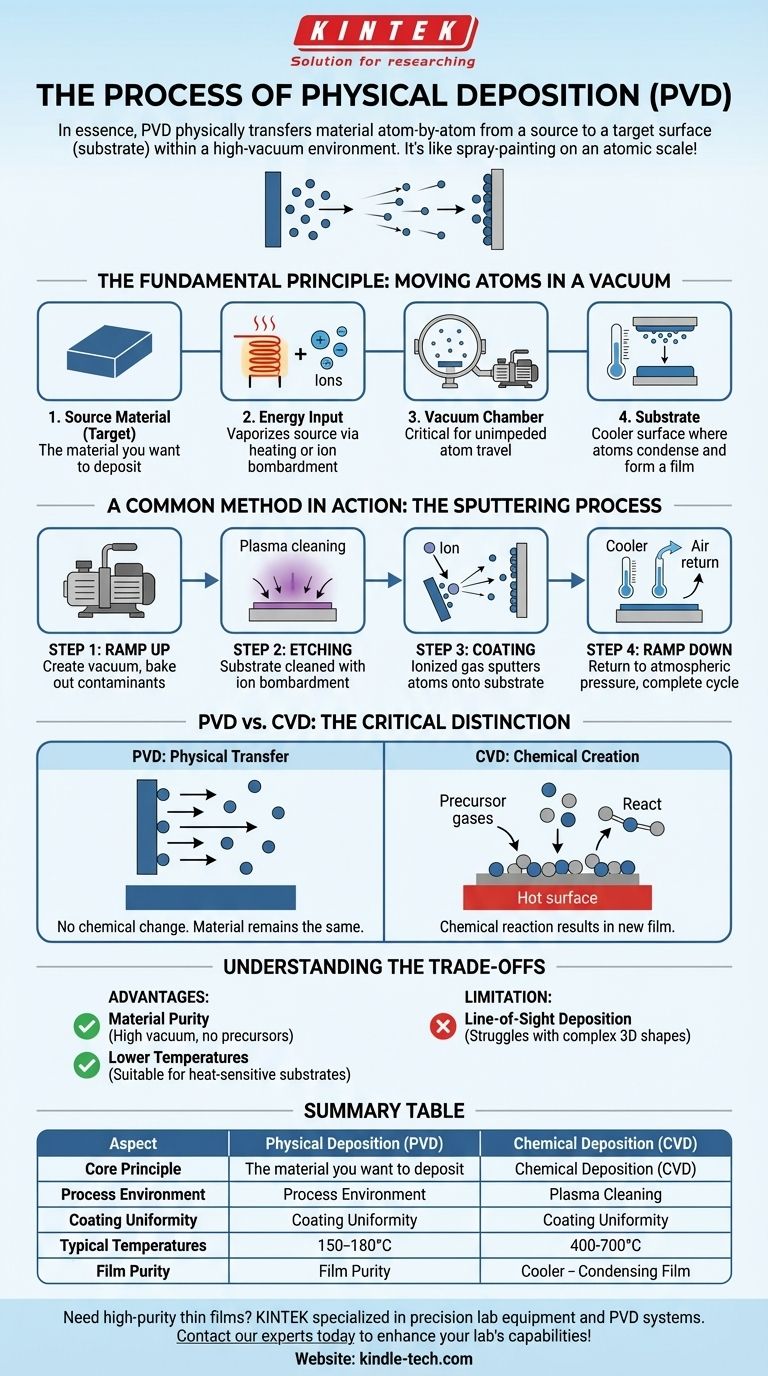
In essence, physical deposition is a process that physically transfers material atom-by-atom from a source to a target surface (a substrate) within a high-vacuum environment. It uses mechanical, electromechanical, or thermodynamic means to vaporize the source material into individual particles. These particles then travel across the vacuum chamber and condense as a thin, solid film onto the cooler substrate.
The core principle of physical deposition is that the deposited material never undergoes a chemical change. It is simply moved from a source to a substrate, much like spray-painting, but on an atomic scale. This distinguishes it from chemical deposition, which builds a film from new materials created by chemical reactions on the substrate's surface.
The Fundamental Principle: Moving Atoms in a Vacuum
Physical Vapor Deposition (PVD) relies on a few core environmental components to function correctly. Understanding these is key to understanding the entire process.
The Source Material
The process begins with a solid source material, often called a "target." This is the exact material you want to deposit as a thin film.
The Energy Input
Energy is applied to this source material to vaporize it. This can be achieved through methods like heating it until it evaporates (thermal evaporation) or bombarding it with high-energy ions to dislodge atoms (sputtering).
The Vacuum Chamber
The entire process occurs inside a vacuum chamber. This vacuum is critical because it removes air and other particles, allowing the vaporized atoms from the source to travel freely to the substrate without colliding with anything else.
The Substrate
This is the object or surface being coated. It is kept at a cooler temperature than the vaporized material, causing the atoms to condense and form a solid, thin layer when they make contact.
A Common Method in Action: The Sputtering Process
Sputtering is a specific and widely used type of physical deposition. It follows a precise, four-step sequence to ensure a high-quality, uncontaminated film.
Step 1: Ramp Up
First, the vacuum chamber is prepared. The pressure is gradually decreased to create a vacuum, while the temperature is often increased to bake out any residual contaminants from the chamber walls.
Step 2: Etching
Before coating, the substrate itself must be perfectly clean. An etching process, often using ions in a plasma, is used to bombard the substrate surface and remove any microscopic contaminations.
Step 3: Coating
This is the core deposition phase. An inert gas (like Argon) is introduced and ionized to create a plasma. These ions are accelerated into the source material, hitting it with enough force to knock off, or "sputter," individual atoms. These liberated atoms then travel through the vacuum and deposit onto the substrate.
Step 4: Ramp Down
Once the desired film thickness is achieved, the coating process is stopped. The chamber is carefully returned to room temperature and normal atmospheric pressure, completing the cycle.
The Critical Distinction: Physical vs. Chemical Deposition
It is crucial not to confuse physical deposition (PVD) with Chemical Vapor Deposition (CVD). While both create thin films, their mechanisms are fundamentally different.
PVD is a Physical Transfer
In PVD, the material of the final film is the same material as the source. Atoms are simply moved from one place to another without a chemical reaction.
CVD is a Chemical Creation
In CVD, one or more gaseous chemical compounds (precursors) are introduced into a chamber. These gases react on the hot substrate surface, undergoing a chemical transformation that results in a solid film being deposited. Unused gases and byproducts are then removed.
Understanding the Trade-offs
Choosing PVD involves recognizing its inherent advantages and limitations compared to other methods.
Advantage: Material Purity
Because PVD is a direct physical transfer in a high vacuum, it is excellent for creating extremely pure films of metals, alloys, and certain ceramics. There are no chemical precursors or byproducts to contaminate the final layer.
Advantage: Lower Temperatures
Many PVD processes can be performed at relatively low temperatures, making them suitable for coating substrates that are sensitive to heat.
Limitation: Line-of-Sight Deposition
The sputtered or evaporated atoms travel in a straight line from the source to the substrate. This "line-of-sight" nature means PVD can struggle to uniformly coat complex, three-dimensional shapes with hidden surfaces or deep trenches.
Making the Right Choice for Your Goal
Selecting the correct deposition method depends entirely on the material you are using and the outcome you need to achieve.
- If your primary focus is creating a high-purity film of a metal or alloy: PVD is often the superior choice due to the direct transfer of material in a clean, vacuum environment.
- If your primary focus is coating a complex 3D object with uniform thickness: CVD is generally more effective, as the precursor gases can flow and react on all exposed surfaces, not just those in the line of sight.
- If you are working with heat-sensitive substrates: The lower operating temperatures of many PVD processes, particularly sputtering, make it a more suitable option.
Ultimately, understanding that physical deposition is a direct, atomic-level transfer process is the key to leveraging its unique advantages.
Summary Table:
| Aspect | Physical Deposition (PVD) | Chemical Deposition (CVD) |
|---|---|---|
| Core Principle | Physical transfer of atoms (no chemical change) | Chemical reaction creates new material on surface |
| Process Environment | High vacuum chamber | Chamber with reactive gases |
| Coating Uniformity | Line-of-sight (challenges with complex 3D shapes) | Excellent for complex 3D shapes (gas flows everywhere) |
| Typical Temperatures | Lower temperatures (good for heat-sensitive substrates) | Higher temperatures often required |
| Film Purity | High purity (direct transfer of source material) | Potential for byproduct contamination |
Need high-purity thin films for your research or production?
KINTEK specializes in precision lab equipment, including PVD systems for depositing pure metal, alloy, and ceramic coatings. Our expertise ensures you get the right solution for your specific substrate and performance requirements.
Contact our experts today to discuss how our PVD technology can enhance your laboratory's capabilities!
Visual Guide
Related Products
- Chemical Vapor Deposition CVD Equipment System Chamber Slide PECVD Tube Furnace with Liquid Gasifier PECVD Machine
- RF PECVD System Radio Frequency Plasma-Enhanced Chemical Vapor Deposition RF PECVD
- 915MHz MPCVD Diamond Machine Microwave Plasma Chemical Vapor Deposition System Reactor
- HFCVD Machine System Equipment for Drawing Die Nano-Diamond Coating
- Customer Made Versatile CVD Tube Furnace Chemical Vapor Deposition Chamber System Equipment
People Also Ask
- What is plasma enhanced chemical vapor deposition PECVD equipment? A Guide to Low-Temperature Thin Film Deposition
- How are carbon nanotubes grown? Master Scalable Production with Chemical Vapor Deposition
- What are the advantages of chemical vapor deposition? Achieve Superior Thin Films for Your Lab
- How expensive is chemical vapor deposition? Understanding the True Cost of High-Performance Coating
- What is the chemical vapor deposition growth process? Build Superior Thin Films from the Atom Up


