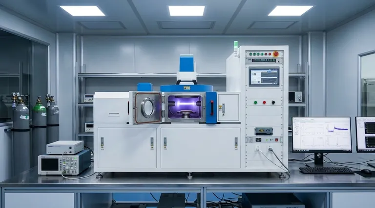
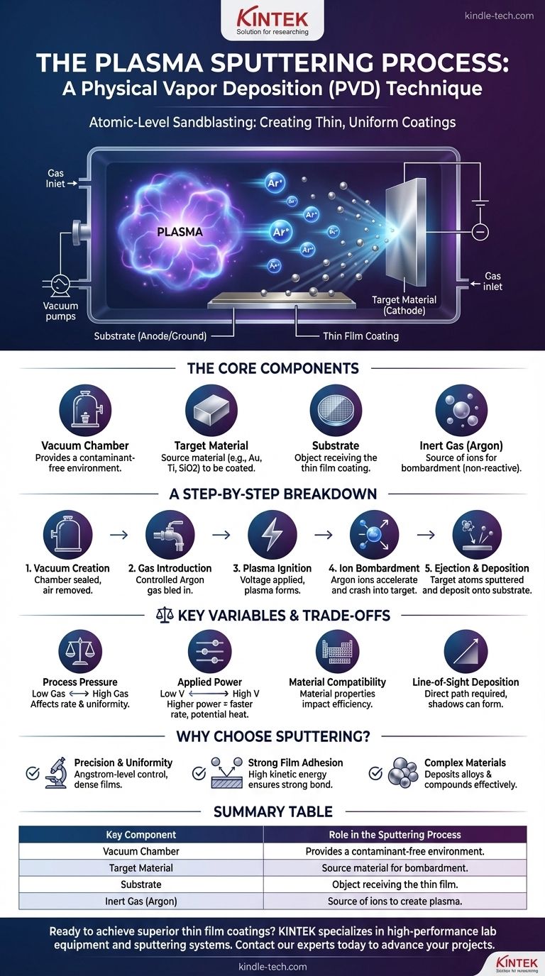
Plasma sputtering is a vacuum deposition technique used to create extremely thin, highly uniform coatings. In this process, a solid material, known as the "target," is bombarded by energetic ions from a plasma, causing atoms to be "sputtered" or ejected from the target's surface. These ejected atoms then travel through the vacuum chamber and deposit onto a substrate, forming a thin film.
At its core, sputtering is a physical process akin to atomic-level sandblasting. It uses ionized gas particles as the abrasive medium to chip atoms off a source material and meticulously deposit them as a high-quality film onto another surface.
The Core Components of a Sputtering System
To understand the process, we must first identify the key players inside the vacuum chamber. Each component has a critical role in achieving the final, precisely engineered coating.
The Vacuum Chamber
The entire process occurs within a sealed chamber from which nearly all air has been removed. This vacuum is essential to prevent the sputtered atoms from colliding with and reacting to air molecules like oxygen and nitrogen, which would contaminate the final film.
The Target Material
This is the source material for the coating. It is a solid block or plate of the substance you wish to deposit, such as titanium, gold, or silicon dioxide. A strong negative voltage is applied to the target.
The Substrate
This is the object or material to be coated. It can be anything from a silicon wafer and glass panel to a plastic component or medical implant. The substrate is strategically placed to intercept the flow of atoms from the target.
The Inert Gas
An inert gas, most commonly Argon (Ar), is introduced into the vacuum chamber in controlled amounts. This gas is not chemically reactive and serves as the source of the ions that will bombard the target.
A Step-by-Step Breakdown of the Process
Sputtering follows a precise sequence of events, transforming a solid target into a thin film through the controlled energy of a plasma.
Step 1: Creating the Vacuum
The chamber is sealed and pumps remove ambient air, creating a high-vacuum environment. This ensures the path from the target to the substrate is clear of contaminants.
Step 2: Introducing the Sputtering Gas
A small, controlled amount of Argon gas is bled into the chamber. The pressure is kept very low but provides enough atoms to sustain the process.
Step 3: Igniting the Plasma
A high voltage is applied, with the target acting as the cathode (negative charge). This electric field energizes the chamber, stripping electrons from the Argon atoms and creating a plasma—a glowing, ionized gas consisting of positive Argon ions (Ar+) and free electrons.
Step 4: Ion Bombardment
The positively charged Argon ions are forcefully accelerated by the electric field and crash into the negatively charged target material with significant kinetic energy.
Step 5: Ejection and Deposition
This high-energy impact transfers momentum from the Argon ion to the target atoms, setting off a collision cascade within the target's surface. When this cascade reaches the surface, target atoms are ejected or "sputtered." These sputtered atoms travel in a straight line until they strike the substrate, where they condense and build up, layer by layer, into a thin film.
Understanding the Trade-offs and Key Variables
The quality and characteristics of the final film are not accidental; they are the result of carefully controlling several process variables. Understanding these trade-offs is key to mastering the technique.
Process Pressure
The amount of inert gas in the chamber affects the sputtering rate and film uniformity. Too little gas means a weak plasma and slow deposition. Too much gas can cause sputtered atoms to scatter, reducing film quality and deposition rate.
Applied Power
Increasing the voltage (power) applied to the target increases the energy of the bombarding ions. This leads to a higher sputtering rate, meaning the film builds up faster. However, excessive power can overheat and damage both the target and the substrate.
Material Compatibility
While sputtering is incredibly versatile, the efficiency of the process depends on the target material's atomic mass and surface binding energy. Heavier ions (like Xenon instead of Argon) can sputter some materials more effectively, but they are also more expensive.
Line-of-Sight Deposition
Sputtering is fundamentally a line-of-sight process. The sputtered atoms travel in straight lines, meaning areas of a complex, three-dimensional substrate that are "in shadow" will not get coated evenly without sophisticated substrate rotation.
Making the Right Choice for Your Goal
Sputtering is chosen over other deposition methods when the application demands superior film quality, adhesion, and control. Your specific goal will determine if it is the optimal approach.
- If your primary focus is precision and uniformity: Sputtering offers exceptional, angstrom-level control over film thickness and produces highly dense, non-porous coatings.
- If your primary focus is strong film adhesion: The high kinetic energy of the sputtered atoms ensures they embed into the substrate surface, creating a more durable and strongly bonded film than other methods like thermal evaporation.
- If your primary focus is depositing complex materials: Sputtering excels at depositing alloys, compounds, and refractory materials while preserving their original chemical composition in the final film.
Ultimately, plasma sputtering is a cornerstone of modern manufacturing, enabling the creation of advanced materials that are essential for everything from microelectronics to durable protective coatings.
Summary Table:
| Key Component | Role in the Sputtering Process |
|---|---|
| Vacuum Chamber | Provides a contaminant-free environment for the deposition process. |
| Target Material | The source material (e.g., gold, titanium) that is bombarded to create the coating. |
| Substrate | The object (e.g., silicon wafer, medical implant) that receives the thin film coating. |
| Inert Gas (Argon) | The ionized gas that creates the plasma to bombard the target. |
Ready to achieve superior thin film coatings for your laboratory?
KINTEK specializes in high-performance lab equipment, including sputtering systems designed for precision, uniformity, and strong adhesion. Whether you're working in microelectronics, materials research, or developing protective coatings, our solutions deliver the reliable results you need.
Contact our experts today to discuss how our sputtering technology can advance your projects and meet your specific laboratory requirements.
Visual Guide
Related Products
- Spark Plasma Sintering Furnace SPS Furnace
- Chemical Vapor Deposition CVD Equipment System Chamber Slide PECVD Tube Furnace with Liquid Gasifier PECVD Machine
- RF PECVD System Radio Frequency Plasma-Enhanced Chemical Vapor Deposition RF PECVD
- Microwave Plasma Chemical Vapor Deposition MPCVD Machine System Reactor for Lab and Diamond Growth
- 915MHz MPCVD Diamond Machine Microwave Plasma Chemical Vapor Deposition System Reactor
People Also Ask
- What is the pressure for spark plasma sintering? A Guide to Optimizing SPS Parameters
- What are the fundamentals of spark plasma sintering process? Unlock Rapid, High-Performance Material Consolidation
- What is the difference between spark plasma sintering and flash sintering? A Guide to Advanced Sintering Methods
- What are the advantages of CAMI/SPS for W-Cu composite preparation? Reduce cycles from hours to seconds.
- What is SPS sintering method? A Guide to High-Speed, High-Performance Material Fabrication


