A thin film production method is a highly controlled process used to deposit an exceptionally thin layer of material onto a surface, known as a substrate. These methods, which include techniques like evaporation, sputtering, and chemical vapor deposition (CVD), give engineers the ability to build up materials layer-by-layer, often at the atomic scale, to achieve specific properties that the bulk material does not possess.
Understanding thin film production is not just about the technique; it's about precisely controlling a material's properties at the atomic level. The chosen deposition method is the critical link between a raw material and its high-tech application, directly determining the film's durability, optical clarity, or electrical conductivity.
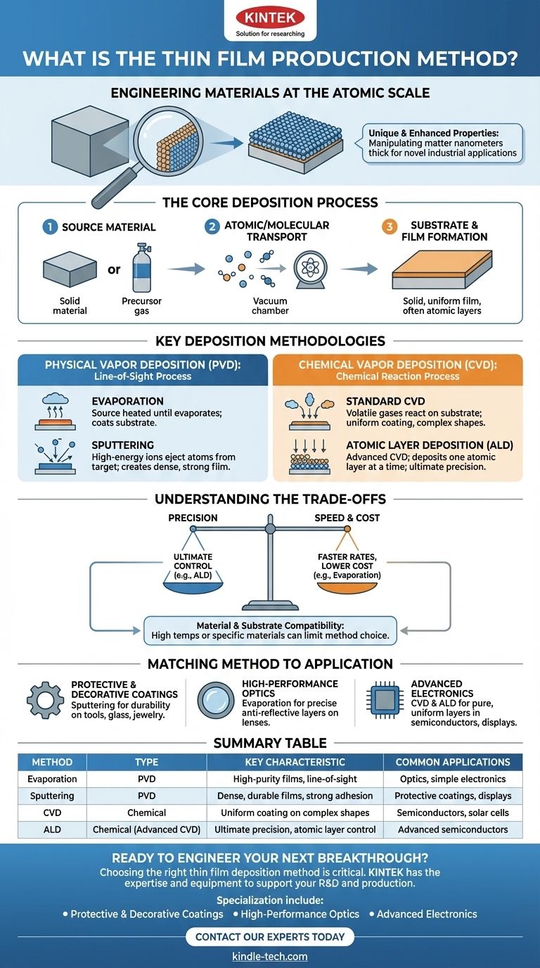
The Goal: From Bulk Material to Atomic Layers
The fundamental purpose of creating a thin film is to engineer a material with unique and enhanced properties. This is achieved by manipulating matter on a microscopic scale.
Why Thin Films Matter
When a material is reduced from its bulk form to a film just nanometers thick, its physical characteristics change dramatically. This is due to an increased surface-area-to-volume ratio and quantum effects, unlocking novel capabilities for a wide range of industrial applications.
The Core Process: Deposition
Nearly all thin film production methods share a common principle. First, a source material is converted into its atomic or molecular components. Then, these particles are transported and deposited onto a substrate within a highly controlled environment, typically a vacuum chamber, to form a solid, uniform film.
Key Deposition Methodologies
The specific method chosen depends entirely on the material being used, the substrate it's being applied to, and the desired properties of the final film. The main categories are Physical Vapor Deposition and Chemical Vapor Deposition.
Physical Vapor Deposition (PVD)
PVD involves physically transforming the solid source material into a vapor that then condenses onto the substrate. This is a "line-of-sight" process where atoms travel directly from the source to the target.
The two most common PVD methods are:
- Evaporation: The source material is heated in a vacuum until it evaporates, creating a vapor that coats the substrate.
- Sputtering: The source material (or "target") is bombarded with high-energy ions, which physically knock atoms off its surface. These ejected atoms then deposit onto the substrate, creating a dense and strongly adhered film.
Chemical Vapor Deposition (CVD)
In CVD, the substrate is exposed to one or more volatile precursor gases. These gases react or decompose on the substrate's surface to produce the desired thin film. This method is not line-of-sight and can coat complex shapes uniformly. Atomic Layer Deposition (ALD) is an advanced form of CVD that deposits material one atomic layer at a time, offering ultimate precision.
Understanding the Trade-offs
No single deposition method is perfect for every application. Choosing the right one requires balancing performance, cost, and material compatibility.
Method Defines the Outcome
The technique used is not arbitrary; it dictates the film's final quality. For instance, sputtered films are often denser and more durable than evaporated films, making them ideal for protective coatings on tools.
Precision vs. Speed and Cost
Highly precise methods like Atomic Layer Deposition offer unparalleled control over film thickness, which is critical for complex semiconductor devices. However, this precision comes at the cost of slower deposition rates and higher equipment expense compared to faster methods like evaporation.
Material and Substrate Limitations
The high temperatures required for some CVD processes can damage sensitive substrates like plastics. Likewise, certain materials are difficult to evaporate or sputter effectively, forcing engineers to choose a method based on chemical and physical compatibility.
Matching the Method to the Application
The ideal production method is dictated entirely by the desired function of the thin film. Your choice will depend on whether you need durability, optical purity, or electrical performance.
- If your primary focus is protective or decorative coatings: Methods like sputtering are often chosen for their durability and strong adhesion on tools, architectural glass, or jewelry.
- If your primary focus is high-performance optics: Processes requiring precise thickness control, such as evaporation or ion beam sputtering, are essential for creating anti-reflective layers on lenses or highly reflective mirrors.
- If your primary focus is advanced electronics: Methods like CVD and ALD are critical for creating the pure, uniform, and complex layers required for semiconductors, solar cells, and touch-panel displays.
By mastering the principles of deposition, we can engineer materials from the atom up, building the foundation for the next generation of technology.
Summary Table:
| Method | Type | Key Characteristic | Common Applications |
|---|---|---|---|
| Evaporation | PVD | High-purity films, line-of-sight | Optics, simple electronics |
| Sputtering | PVD | Dense, durable films, strong adhesion | Protective coatings, displays |
| CVD | Chemical | Uniform coating on complex shapes | Semiconductors, solar cells |
| ALD | Chemical (Advanced CVD) | Ultimate precision, atomic layer control | Advanced semiconductors |
Ready to Engineer Your Next Breakthrough?
Choosing the right thin film deposition method is critical to your product's performance, durability, and cost. Whether you need durable protective coatings, high-precision optical layers, or complex electronic films, KINTEK has the expertise and equipment to support your R&D and production.
We specialize in providing lab equipment and consumables for:
- Protective & Decorative Coatings: Achieve superior hardness and adhesion.
- High-Performance Optics: Create precise anti-reflective or reflective layers.
- Advanced Electronics: Develop the pure, uniform films required for semiconductors and displays.
Let's discuss your specific material and substrate requirements. Contact our experts today to find the optimal thin film solution for your application.
Visual Guide
Related Products
- CVD Diamond Dressing Tools for Precision Applications
- Multi Heating Zones CVD Tube Furnace Machine Chemical Vapor Deposition Chamber System Equipment
- CVD Diamond Domes for Industrial and Scientific Applications
- CVD Diamond for Thermal Management Applications
- Chemical Vapor Deposition CVD Equipment System Chamber Slide PECVD Tube Furnace with Liquid Gasifier PECVD Machine
People Also Ask
- How do you identify a CVD diamond? The Definitive Guide to Lab-Grown Diamond Verification
- What is chemical vapor deposition of diamond? Grow High-Purity Diamonds Atom-by-Atom
- How long does it take to make synthetic diamonds? Discover the 6-8 Week Science Behind Lab-Grown Gems
- How do CVD diamonds grow? A Step-by-Step Guide to Lab-Grown Diamond Creation
- What color diamonds are CVD? Understanding the Process from Brown Tint to Colorless Beauty


