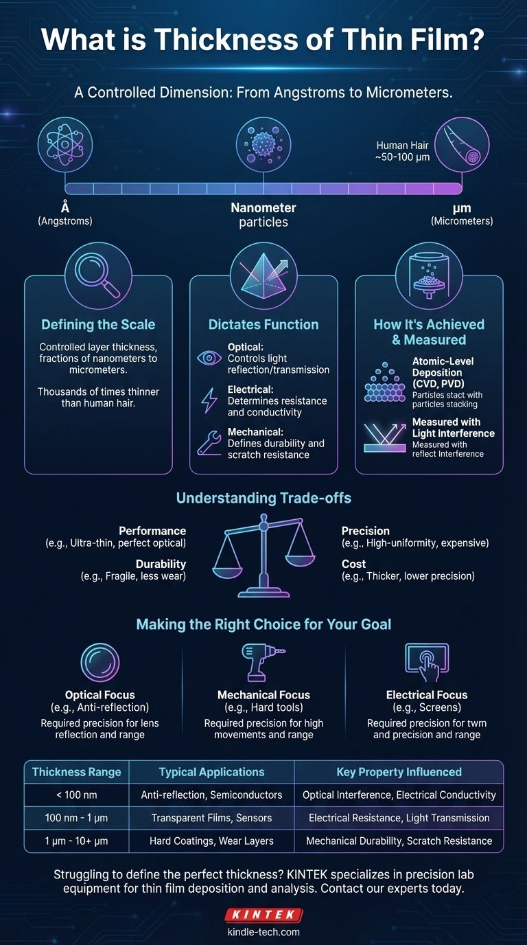
A thin film's thickness is not a single value but a controlled dimension that typically ranges from a few angstroms (fractions of a nanometer) to several micrometers. This thickness is the most critical parameter that defines the film's optical, electrical, and mechanical properties, making it a fundamental aspect of its design and function.
The concept of "thin film" describes a vast category of material layers where the thickness is a deliberate engineering choice. It's less about a specific number and more about using a precise, microscopic dimension to achieve a specific physical effect.
Defining the Scale of "Thin"
To understand thin films, we must first grasp the microscopic scale we are operating on. The specified thickness is directly tied to the film's intended purpose.
From Nanometers to Micrometers
A thin film is a layer of material deposited onto a substrate. Its thickness can be as small as a fraction of a nanometer (a few angstroms) or extend up to several micrometers (microns).
To put this in perspective, a human hair is about 50-100 micrometers thick. The thickest thin films are still many times thinner than a single hair, and the thinnest are thousands of times thinner.
Why Thickness Dictates Function
The specific thickness is chosen to manipulate physical phenomena. For example, a film's ability to reflect or transmit light is directly dependent on its thickness relative to the wavelength of that light.
Similarly, a film's electrical resistance or its durability against scratches is a direct function of how much material is present—a property controlled by its thickness.
How Thickness is Achieved and Measured
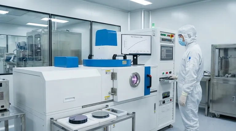
Creating and verifying layers this thin requires incredibly precise technology. The methods used highlight why thickness is a result of careful design, not a byproduct.
Atomic-Level Deposition
Techniques like Chemical Vapor Deposition (CVD) and Physical Vapor Deposition (PVD) are used to build these films. These processes deposit material literally one layer of atoms or molecules at a time.
This atomic-level control is what allows engineers to specify a thickness down to the nanometer to achieve a desired outcome.
Measuring with Light
The most common way to measure the thickness of a transparent thin film is by analyzing light. A beam of light is used to create an interference pattern from the reflections off the top and bottom surfaces of the film.
By analyzing this pattern of light waves, engineers can calculate the film's thickness with extreme precision. This method requires knowing the material's refractive index, as light travels through different materials at different speeds.
Understanding the Trade-offs
Choosing a film's thickness is a balancing act between performance, durability, and cost. The "right" thickness is always relative to the application's goals and constraints.
Performance vs. Durability
An ultra-thin film might offer perfect optical performance for an anti-reflection coating but be too fragile for a high-wear environment.
Conversely, a thicker film designed for scratch resistance might be very durable but could slightly alter the optical clarity or color of the underlying substrate.
Precision vs. Cost
Achieving a highly uniform film with single-nanometer precision requires sophisticated and expensive deposition and monitoring equipment.
For applications where such precision isn't necessary, like a simple decorative metal coating on glass, less complex methods can be used to create thicker films at a lower cost.
Making the Right Choice for Your Goal
The ideal thickness of a thin film is determined entirely by its application. Consider the primary goal to understand the required scale.
- If your primary focus is optical performance (e.g., anti-reflection lenses): Thickness must be controlled with nanometer-level precision to interfere with specific wavelengths of light.
- If your primary focus is mechanical protection (e.g., hard coating on tools): A thicker film, often in the micrometer range, is necessary to provide durability and wear resistance.
- If your primary focus is electrical function (e.g., transparent conductors on a screen): Thickness is carefully selected to achieve a target electrical resistance, balancing conductivity with transparency.
Ultimately, a thin film's thickness is the primary tool an engineer uses to control the physics of a surface.
Summary Table:
| Thickness Range | Typical Applications | Key Property Influenced |
|---|---|---|
| < 100 nm (Nanometers) | Anti-reflection coatings, semiconductor layers | Optical interference, electrical conductivity |
| 100 nm - 1 μm | Transparent conductive films, sensor layers | Electrical resistance, light transmission |
| 1 μm - 10+ μm (Micrometers) | Hard protective coatings, wear-resistant layers | Mechanical durability, scratch resistance |
Struggling to define the perfect thin film thickness for your project's optical, electrical, or mechanical requirements? KINTEK specializes in precision lab equipment and consumables for thin film deposition and analysis. Our expertise helps you achieve the exact nanometer or micrometer-scale control needed for superior performance and durability. Contact our experts today to discuss your specific application and discover the right solution for your laboratory needs.
Visual Guide
Related Products
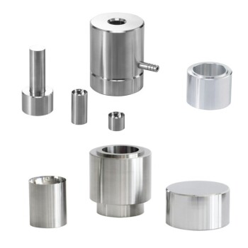
- RF PECVD System Radio Frequency Plasma-Enhanced Chemical Vapor Deposition RF PECVD
- Chemical Vapor Deposition CVD Equipment System Chamber Slide PECVD Tube Furnace with Liquid Gasifier PECVD Machine
- Molybdenum Tungsten Tantalum Evaporation Boat for High Temperature Applications
- Hemispherical Bottom Tungsten Molybdenum Evaporation Boat
- Aluminized Ceramic Evaporation Boat for Thin Film Deposition
People Also Ask
- What is the principle of plasma enhanced chemical vapor deposition? Achieve Low-Temperature Thin Film Deposition
- What are the applications of PECVD? Essential for Semiconductors, MEMS, and Solar Cells
- Why is PECVD environment friendly? Understanding the Eco-Friendly Benefits of Plasma-Enhanced Coating
- What is an example of PECVD? RF-PECVD for High-Quality Thin Film Deposition
- How does RF power create plasma? Achieve Stable, High-Density Plasma for Your Applications