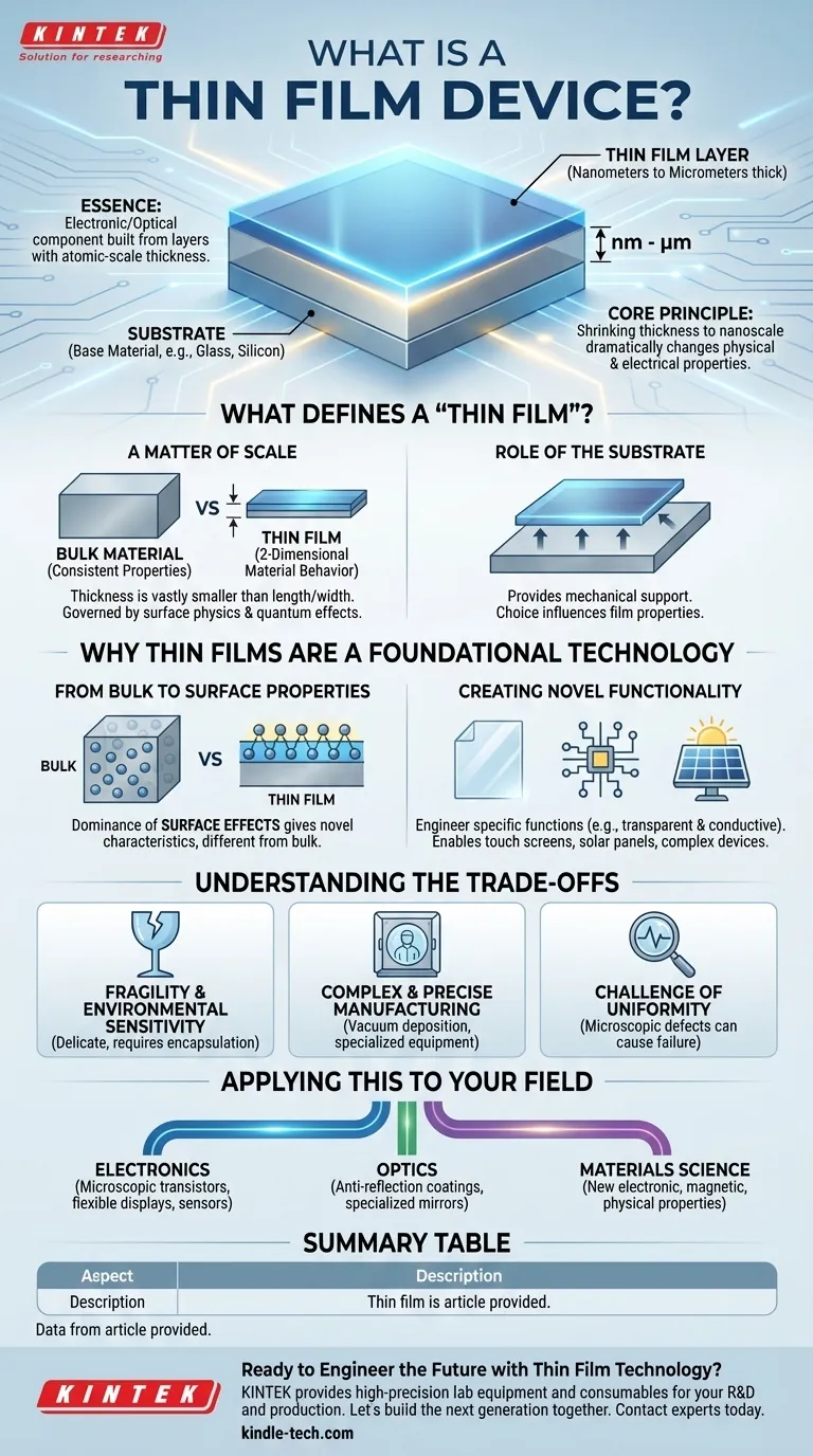
In essence, a thin film device is an electronic or optical component built from one or more layers of material that are exceptionally thin. These layers, often deposited onto a supportive base called a substrate, have a thickness measured in nanometers (billionths of a meter) or micrometers (millionths of a meter), allowing for the creation of unique and complex functionalities.
The core principle of thin film technology is that by shrinking a material's thickness to an atomic scale, its physical and electrical properties change dramatically. We suppress the material's third dimension to unlock new capabilities in the other two.
What Defines a "Thin Film"?
To understand the device, you must first understand the film itself. It is defined not just by what it is, but by its extreme dimensions.
A Matter of Scale
A material is considered a thin film when its thickness is vastly smaller than its length and width. This thickness ranges from a few micrometers down to a single layer of atoms (a monolayer).
At this scale, the film effectively behaves like a 2-dimensional material. Its properties are no longer governed by the bulk characteristics of the substance but by surface physics and quantum effects.
The Role of the Substrate
Thin films are not freestanding; they are almost always deposited onto a substrate. This is a base material, like glass, silicon, or flexible plastic, that provides mechanical support.
The choice of substrate is critical, as it can influence the properties of the film grown upon it.
Why Thin Films Are a Foundational Technology
The entire purpose of creating thin films is to harness the unique properties that emerge at this minuscule scale.
From Bulk to Surface Properties
In a normal, "bulk" material, the vast majority of atoms are surrounded by other atoms, and its properties (like conductivity or color) are consistent.
In a thin film, a significant percentage of atoms are on the surface or near an interface. This dominance of surface effects is what gives thin films their novel characteristics, which are often completely different from their bulk counterparts.
Creating Novel Functionality
This shift in properties allows us to engineer materials with specific functions. For example, we can create a material that is both electrically conductive and optically transparent, a combination impossible in most bulk materials.
This is the basis for touch screens, solar panels, and modern flat-panel displays. Stacking different thin films allows for the creation of complex devices like transistors or memory cells.
Understanding the Trade-offs
While powerful, thin film technology comes with inherent challenges that define its application and manufacturing.
Fragility and Environmental Sensitivity
By their very nature, thin films are delicate. They can be susceptible to scratches, mechanical stress, and degradation from exposure to air or moisture. Protecting them often requires additional encapsulation layers.
Complex and Precise Manufacturing
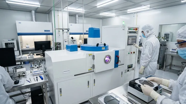
Depositing a perfectly uniform film that is only a few hundred atoms thick requires highly controlled conditions. Processes like vacuum deposition or chemical vapor deposition demand specialized, expensive equipment and cleanroom environments.
The Challenge of Uniformity
Achieving a flawless film over a large area is a significant engineering hurdle. Even microscopic defects like pinholes or variations in thickness can cause a device to fail completely.
Applying This to Your Field
Your perspective on thin film devices will depend on your specific goal.
- If your primary focus is electronics: Think of thin films as the method for building microscopic transistors and circuits on substrates like glass or plastic, enabling flexible displays and large-area sensors.
- If your primary focus is optics: View thin films as a tool to precisely control light, creating everything from anti-reflection coatings on your glasses to highly specialized mirrors for lasers.
- If your primary focus is materials science: See thin films as a gateway to creating engineered materials with entirely new electronic, magnetic, or physical properties not found in nature.
Ultimately, thin film technology is about manipulating matter at its most fundamental level to engineer the future of electronics and materials.
Summary Table:
| Aspect | Description |
|---|---|
| Definition | An electronic/optical component built from layers nanometers to micrometers thick on a substrate. |
| Key Principle | At nanoscale thickness, material properties shift from bulk to surface-dominated, enabling new functionalities. |
| Common Applications | Transistors, solar panels, touch screens, anti-reflection coatings, specialized mirrors. |
| Key Challenges | Fragility, complex manufacturing (e.g., vacuum deposition), and achieving perfect uniformity. |
Ready to Engineer the Future with Thin Film Technology?
Thin film devices are the foundation of modern innovation, from flexible electronics to advanced optics. KINTEK specializes in providing the high-precision lab equipment and consumables essential for your thin film R&D and production. Whether you are developing new materials or scaling up manufacturing, our solutions ensure the precision and reliability you need.
Let's build the next generation of technology together. Contact our experts today to discuss how KINTEK can support your laboratory's specific thin film challenges.
Visual Guide
Related Products
- RF PECVD System Radio Frequency Plasma-Enhanced Chemical Vapor Deposition RF PECVD
- Chemical Vapor Deposition CVD Equipment System Chamber Slide PECVD Tube Furnace with Liquid Gasifier PECVD Machine
- Molybdenum Tungsten Tantalum Evaporation Boat for High Temperature Applications
- Hemispherical Bottom Tungsten Molybdenum Evaporation Boat
- Aluminized Ceramic Evaporation Boat for Thin Film Deposition
People Also Ask
- What are the applications of PECVD? Essential for Semiconductors, MEMS, and Solar Cells
- What is plasma activated chemical vapour deposition method? A Low-Temperature Solution for Advanced Coatings
- How are PECVD and CVD different? A Guide to Choosing the Right Thin-Film Deposition Process
- Why does PECVD commonly use RF power input? For Precise Low-Temperature Thin Film Deposition
- Why is PECVD environment friendly? Understanding the Eco-Friendly Benefits of Plasma-Enhanced Coating