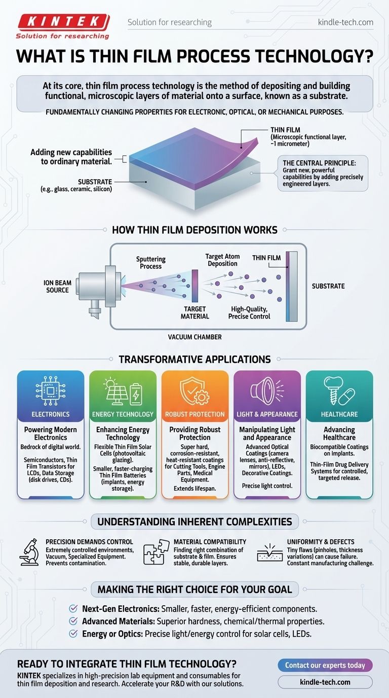
At its core, thin film process technology is the method of depositing and building functional, microscopic layers of material onto a surface, known as a substrate. These films can be as thin as a single micrometer (1/1000th of a millimeter) and are constructed by stacking layer upon layer. This process is not just about making things smaller; it’s about fundamentally changing the properties of the base material to serve a specific electronic, optical, or mechanical purpose.
The central principle of thin film technology is to grant new, powerful capabilities to an ordinary material. By adding precisely engineered microscopic layers, a simple piece of glass or ceramic can be transformed into a solar panel, a computer chip, or a self-sterilizing surface.
How Thin Film Deposition Works
Thin film technology is less a single method and more a category of highly controlled manufacturing processes. The underlying concept, however, remains consistent.
The Core Principle: Substrate and Film
Every application begins with a substrate, which is the base material (like ceramic, silicon, or plastic). The goal is to add one or more thin films to this substrate. Each film is a layer of a different material, chosen for a specific property like electrical conductivity, light reflection, or hardness.
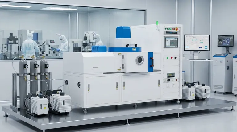
A Key Deposition Method: Sputtering
One common and highly precise method is ion beam sputtering. In this process, a beam of ions is fired at a "target" material. This impact knocks atoms off the target, which then travel and deposit themselves in a uniform layer on the substrate, forming a high-quality, precisely controlled thin film.
The Transformative Applications of Thin Films
The ability to add new functionality to surfaces has enabled breakthroughs across nearly every modern industry. The applications are defined by the properties of the deposited films.
Powering Modern Electronics
Thin films are the bedrock of the digital world. They are used to create the intricate circuits on semiconductors, the tiny components in thin film transistors that power vivid LCD screens, and the magnetic layers on disk drives and CDs that store our data.
Enhancing Energy Technology
This technology is crucial for green energy. Thin film solar cells are flexible and lightweight, making them ideal for new applications like photovoltaic glazing on buildings. Similarly, thin film batteries can be made smaller, more efficient, and faster-charging, improving everything from medical implants to large-scale energy storage.
Providing Robust Protection
Many films are deposited for their mechanical properties. They create super hard, corrosion-resistant, and heat-resistant coatings on cutting tools, engine parts, and medical equipment, dramatically extending the lifespan and performance of these items.
Manipulating Light and Appearance
Thin films can be engineered to control light with incredible precision. This is the basis for advanced optical coatings on camera lenses, anti-reflective coatings on eyeglasses, the production of mirrors, and the light-emitting layers within LEDs. This also extends to decorative coatings on consumer products.
Advancing Healthcare
Beyond protecting equipment, thin films are enabling new medical treatments. This includes biocompatible coatings on implants and the development of thin-film drug delivery systems that can release medicine in a controlled, targeted manner.
Understanding the Inherent Complexities
While incredibly powerful, thin film technology is not a simple process. Its precision and scale present significant engineering challenges that are important to understand.
Precision Demands Control
Depositing a perfectly uniform layer just a few atoms thick requires an extremely controlled environment. These processes often take place in a vacuum and demand specialized, expensive equipment to prevent contamination and ensure consistency.
Material Compatibility is Key
Not every film material will adhere properly to every substrate. A great deal of materials science research is dedicated to finding the right combination of substrate, film materials, and deposition process to ensure the layers are stable and durable.
Uniformity and Defects
At the microscopic level, even a tiny flaw—like a pinhole or a slight variation in thickness—can cause an entire electronic component or optical filter to fail. Achieving near-perfect uniformity across the entire surface of the substrate is a constant manufacturing challenge.
Making the Right Choice for Your Goal
Understanding thin film technology allows you to see it as a foundational tool for innovation. How you leverage it depends entirely on your end goal.
- If your primary focus is creating next-generation electronics: This technology is your key to making components smaller, faster, and more energy-efficient.
- If your primary focus is developing advanced materials: Use this process to create surfaces with superior hardness, chemical resistance, or thermal properties that were previously impossible.
- If your primary focus is innovating in energy or optics: Leverage thin films to precisely control light and energy conversion for applications like high-efficiency solar cells, LEDs, and specialized lenses.
Ultimately, thin film technology is a cornerstone of modern engineering, allowing us to build function and intelligence onto the very surface of materials.
Summary Table:
| Application Area | Key Function of Thin Film | Common Examples |
|---|---|---|
| Electronics | Create micro-circuits and transistors | Semiconductors, LCD screens |
| Energy | Enable light-to-energy conversion and storage | Thin film solar cells, advanced batteries |
| Protective Coatings | Add hardness and corrosion resistance | Cutting tools, medical equipment |
| Optics | Precisely control light reflection/transmission | Camera lenses, anti-reflective coatings, LEDs |
| Healthcare | Provide biocompatibility and controlled drug release | Medical implants, drug delivery systems |
Ready to integrate thin film technology into your next innovation?
KINTEK specializes in providing high-precision lab equipment and consumables for thin film deposition and research. Whether you are developing advanced semiconductors, next-generation solar cells, or specialized optical coatings, our solutions help you achieve the material properties and performance you need.
Contact our experts today to discuss how our equipment can accelerate your R&D and manufacturing processes.
Visual Guide
Related Products
- Aluminized Ceramic Evaporation Boat for Thin Film Deposition
- Tungsten Evaporation Boat for Thin Film Deposition
- Electron Beam Evaporation Coating Oxygen-Free Copper Crucible and Evaporation Boat
- Molybdenum Tungsten Tantalum Evaporation Boat for High Temperature Applications
- HFCVD Machine System Equipment for Drawing Die Nano-Diamond Coating
People Also Ask
- Why is an alumina boat and Ti3AlC2 powder bed necessary for Ti2AlC sintering? Protect MAX Phase Purity
- What is the chemical method for thin film deposition? Build Films from the Molecular Level Up
- Why is an alumina boat selected for catalyst precursors? Ensure Sample Purity at 1000 °C
- What is the widely used boat made of in thermal evaporation? Choosing the Right Material for High-Purity Deposition
- What are the alternatives to sputtering? Choose the Right Thin Film Deposition Method


