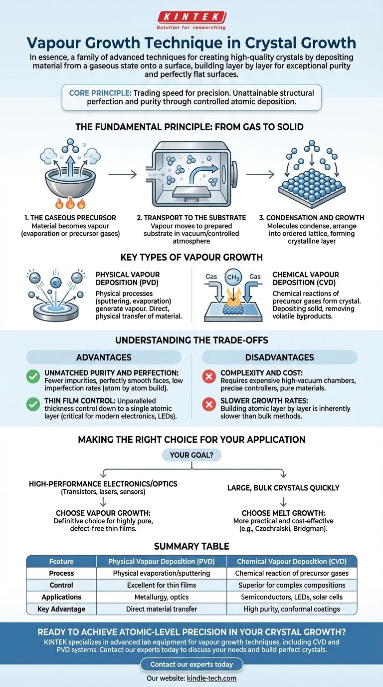
In essence, vapour growth is a family of advanced techniques for creating high-quality crystals by depositing material from a gaseous state onto a surface. Unlike methods that grow crystals from a liquid melt, this process builds the crystal layer by layer, often atom by atom, resulting in structures with exceptional purity and perfectly flat surfaces ideal for modern electronics and materials science.
The core principle of vapour growth is trading speed for precision. By carefully controlling the deposition of gaseous atoms or molecules onto a substrate, this technique achieves a level of structural perfection and purity that is unattainable with faster, bulk-growth methods.
The Fundamental Principle: From Gas to Solid
Vapour growth techniques are all based on a three-step phase transition process, moving from a gas to a highly ordered solid.
The Gaseous Precursor
First, the material intended for crystal growth must exist as a vapour. This can be achieved by heating a solid or liquid source until it evaporates or by using precursor gases that will react to form the desired material.
Transport to the Substrate
This vapour is then transported, typically within a vacuum or controlled-atmosphere chamber, to a prepared surface called a substrate. The substrate acts as the foundation upon which the new crystal will form.
Condensation and Growth
When the hot gas molecules or atoms make contact with the cooler substrate, they lose energy, slow down, and condense. Under precisely controlled conditions, these atoms arrange themselves into a repeating, ordered lattice, creating a high-quality crystalline layer.
Key Types of Vapour Growth
While the principle is the same, the methods for creating and depositing the vapour fall into two main categories.
Physical Vapour Deposition (PVD)
PVD involves physical processes to generate the vapour. A solid "target" material is bombarded with high-energy ions (sputtering) or heated in a vacuum until it evaporates. The resulting vapour then travels in a straight line and condenses on the substrate. This is a direct, physical transfer of material.
Chemical Vapour Deposition (CVD)
CVD uses chemical reactions to form the crystal. One or more precursor gases are introduced into a reaction chamber. These gases decompose or react on the hot substrate surface, depositing the desired solid material and forming volatile byproducts that are then removed.
Understanding the Trade-offs
Choosing a growth technique requires a clear understanding of its inherent advantages and disadvantages. Vapour growth is powerful but not universally applicable.
The Advantage: Unmatched Purity and Perfection
Because the material is built atom by atom, there are far fewer opportunities for impurities or structural defects to become trapped in the crystal lattice. This is why vapour growth produces crystals with perfectly smooth faces and low imperfection rates, as mentioned in the reference materials.
The Advantage: Thin Film Control
This technique offers unparalleled control over thickness, down to a single atomic layer. This precision is absolutely critical for manufacturing modern semiconductor devices, LEDs, solar cells, and protective coatings.
The Disadvantage: Complexity and Cost
Vapour growth systems often require expensive high-vacuum chambers, precise temperature and gas flow controllers, and pure precursor materials. The initial investment and operating costs are significantly higher than for many bulk growth methods.
The Disadvantage: Slower Growth Rates
Building a crystal one atomic layer at a time is inherently slower than pulling a large crystal from a pool of molten liquid. For applications requiring large, bulk crystals, vapour growth is often impractical due to the time required.
Making the Right Choice for Your Application
The decision to use vapour growth hinges entirely on your end goal, balancing the need for quality against the constraints of speed and cost.
- If your primary focus is high-performance electronics or optics: Vapour growth is the definitive choice for creating the highly pure, defect-free thin films required for transistors, lasers, and sensors.
- If your primary focus is producing large, bulk crystals quickly: Melt growth techniques (like the Czochralski or Bridgman methods) are almost always more practical and cost-effective.
Ultimately, choosing vapour growth is a decision to prioritize structural perfection and atomic-level control above all else.
Summary Table:
| Feature | Physical Vapour Deposition (PVD) | Chemical Vapour Deposition (CVD) |
|---|---|---|
| Process | Physical evaporation/sputtering | Chemical reaction of precursor gases |
| Control | Excellent for thin films | Superior for complex compositions |
| Applications | Metallurgy, optics | Semiconductors, LEDs, solar cells |
| Key Advantage | Direct material transfer | High purity, conformal coatings |
Ready to achieve atomic-level precision in your crystal growth?
KINTEK specializes in advanced lab equipment for vapour growth techniques, including CVD and PVD systems. Whether you're developing next-generation semiconductors, high-efficiency solar cells, or specialized optical coatings, our solutions deliver the unmatched purity and thin-film control your research demands.
Contact our experts today to discuss how we can support your laboratory's specific vapour growth needs and help you build the perfect crystals for your application.
Visual Guide
Related Products
- CVD Diamond Dressing Tools for Precision Applications
- Multi Heating Zones CVD Tube Furnace Machine Chemical Vapor Deposition Chamber System Equipment
- CVD Diamond Domes for Industrial and Scientific Applications
- CVD Diamond for Thermal Management Applications
- Chemical Vapor Deposition CVD Equipment System Chamber Slide PECVD Tube Furnace with Liquid Gasifier PECVD Machine
People Also Ask
- What are the disadvantages of CVD diamonds? Understanding the trade-offs for your purchase.
- How do CVD diamonds grow? A Step-by-Step Guide to Lab-Grown Diamond Creation
- What is CVD diamond? The Ultimate Guide to Lab-Grown Diamonds and Their Uses
- What are the raw materials for CVD diamonds? A seed, a gas, and the science of crystal growth.
- Can CVD diamonds change color? No, their color is permanent and stable.


