The definitive technique for depositing ultra-thin films with atomic layer precision is Atomic Layer Deposition (ALD). Unlike other methods that deposit material continuously, ALD is a cyclical process that builds films one single atomic layer at a time. This self-limiting nature gives it unparalleled control over film thickness and uniformity, down to the single-angstrom level.
Atomic Layer Deposition (ALD) achieves its precision not through speed, but through a fundamentally different, self-terminating chemical process. This makes it the only viable method when perfect conformity and atomic-scale control are non-negotiable requirements.
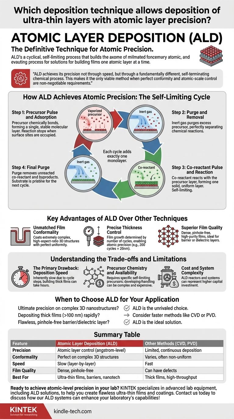
How ALD Achieves Atomic Precision: The Self-Limiting Cycle
The power of ALD comes from its unique four-step process, which is repeated in cycles to build up a film. Each cycle adds exactly one monolayer of material, guaranteeing precision. This process relies on separating two chemical half-reactions in time.
Step 1: Precursor Pulse and Adsorption
First, a vaporized chemical, known as the precursor, is pulsed into the deposition chamber. This precursor chemically bonds (chemisorbs) to the surface of the substrate, forming a single, stable molecular layer. The reaction naturally stops once all available surface sites are occupied.
Step 2: Purge and Removal
Next, an inert gas like nitrogen or argon is used to purge the chamber. This step is critical, as it removes any excess precursor molecules that did not react with the surface. This ensures that the two chemical reactions are perfectly separated.
Step 3: Co-reactant Pulse and Reaction
A second chemical, the co-reactant (often water, ozone, or plasma), is then pulsed into the chamber. It reacts with the precursor layer already on the surface, completing the chemical reaction and forming one solid, uniform layer of the desired material. This reaction is also self-limiting.
Step 4: Final Purge
A final purge with inert gas removes any unreacted co-reactant and gaseous byproducts from the reaction. The substrate surface is now pristine and ready for the next cycle to begin, allowing another atomic layer to be deposited on top of the first.
Key Advantages of ALD Over Other Techniques
While other deposition methods like Chemical Vapor Deposition (CVD) or Physical Vapor Deposition (PVD) exist, ALD offers unique benefits for high-precision applications.
Unmatched Film Conformality
Because the process relies on gaseous chemicals reaching every part of a surface before reacting, ALD can coat extremely complex, high-aspect-ratio 3D structures with perfect uniformity. The film thickness will be identical on the top, bottom, and sidewalls of a microscopic trench.
Precise Thickness Control
Since film growth is determined by the number of cycles performed, thickness can be controlled with atomic precision. If one cycle deposits 0.1 nanometers (1 angstrom) of material, 200 cycles will deposit exactly 20 nanometers. This level of digital control is impossible with other methods.
Superior Film Quality
ALD can often be performed at lower temperatures than CVD. The self-limiting, layer-by-layer growth results in films that are incredibly dense, pinhole-free, and of high purity, making them excellent for use as barrier or dielectric layers.
Understanding the Trade-offs and Limitations
No technique is perfect, and ALD's precision comes at a cost. Understanding its drawbacks is essential for making an informed decision.
The Primary Drawback: Deposition Speed
ALD is inherently slow. Because each cycle deposits only a fraction of a nanometer and involves multiple pulse and purge steps, building up a thick film can take hours. Methods like CVD are orders of magnitude faster, making them better suited for applications where thickness is more important than precision.
Precursor Chemistry and Availability
The success of ALD is entirely dependent on having the right pair of chemical precursors that exhibit ideal self-limiting behavior. Developing, synthesizing, and handling these chemicals can be complex and expensive. Some materials simply do not have a known, effective ALD process.
Cost and System Complexity
While becoming more common, ALD reactors and their associated vacuum and chemical delivery systems can represent a higher capital investment compared to some simpler PVD or wet-chemical deposition systems.
When to Choose ALD for Your Application
Selecting the right deposition technique requires balancing the need for precision against the practical constraints of speed and cost.
- If your primary focus is ultimate precision on complex 3D nanostructures: ALD is the unrivaled choice and often the only technology that can meet the requirement.
- If your primary focus is depositing thick films (>100 nm) rapidly: You should strongly consider faster methods like CVD or PVD, as ALD will be too slow.
- If your primary focus is creating a flawless, pinhole-free barrier or dielectric layer: ALD is the ideal solution due to its dense, uniform, and conformal film growth.
Ultimately, understanding the fundamental trade-off between the digital precision of ALD and the analog speed of other methods is the key to successful materials engineering.
Summary Table:
| Feature | Atomic Layer Deposition (ALD) | Other Methods (CVD, PVD) |
|---|---|---|
| Precision | Atomic layer control (angstrom-level) | Limited, continuous deposition |
| Conformality | Perfect on complex 3D structures | Varies, often non-uniform |
| Speed | Slow (layer-by-layer) | Fast |
| Film Quality | Dense, pinhole-free | Can have defects |
| Best For | Ultra-thin films, barriers, nanotech | Thick films, high-throughput |
Ready to achieve atomic-level precision in your lab? KINTEK specializes in advanced lab equipment, including ALD solutions, to help you create flawless ultra-thin films and coatings. Whether you're working on nanotechnology, semiconductors, or advanced materials, our expertise ensures you get the perfect conformity and control your research demands. Contact us today to discuss how our ALD systems can enhance your laboratory's capabilities!
Visual Guide
Related Products
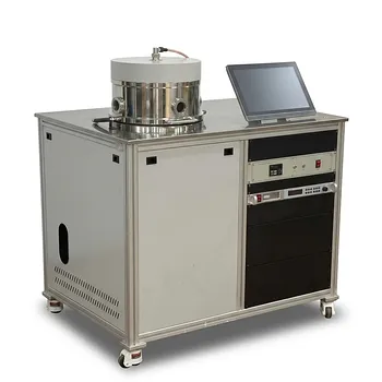
- RF PECVD System Radio Frequency Plasma-Enhanced Chemical Vapor Deposition RF PECVD
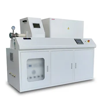
- Inclined Rotary Plasma Enhanced Chemical Vapor Deposition PECVD Equipment Tube Furnace Machine
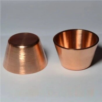
- Electron Beam Evaporation Coating Oxygen-Free Copper Crucible and Evaporation Boat
- Chemical Vapor Deposition CVD Equipment System Chamber Slide PECVD Tube Furnace with Liquid Gasifier PECVD Machine
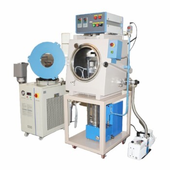
- Vacuum Hot Press Furnace Machine for Lamination and Heating
People Also Ask
- What is plasma activated chemical vapour deposition method? A Low-Temperature Solution for Advanced Coatings
- What is the speed of PECVD? Achieve High-Speed, Low-Temperature Deposition for Your Lab
- Why does PECVD commonly use RF power input? For Precise Low-Temperature Thin Film Deposition
- What are the advantages of plasma enhanced CVD? Enable Low-Temperature, High-Quality Thin Film Deposition
- What are the benefits of PECVD? Achieve Superior Low-Temperature Thin Film Deposition

