In short, thin films are useful because they allow us to engineer the surface properties of a material without changing the bulk material itself. This provides a vast range of benefits, from enhanced durability and corrosion resistance to unique optical and electrical functionalities, making them critical in industries from aerospace to consumer electronics.
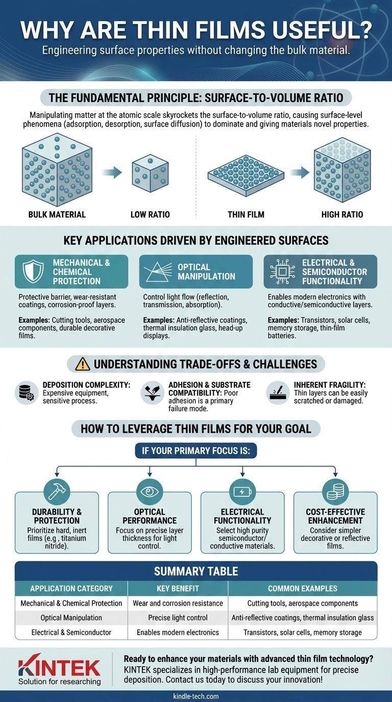
The true power of thin films lies in manipulating matter at the atomic scale. By creating layers only a few atoms or molecules thick, the surface-to-volume ratio skyrockets, causing surface-level phenomena to dominate and granting materials novel properties they simply do not possess in their bulk form.
The Fundamental Principle: Why Size Changes Everything
To grasp why thin films are so transformative, you must first understand that a material's properties can change dramatically when it is reduced to a nanometer-scale thickness.
The Power of the Surface-to-Volume Ratio
In a large, bulk object, most atoms are on the inside, surrounded by other atoms. Only a tiny fraction are on the surface.
In a thin film, a massive proportion of the atoms are on the surface or very close to it. This radical shift in the surface-to-volume ratio is the key.
The Dominance of Surface Phenomena
Because so many atoms are on the surface, phenomena that are negligible in bulk materials become dominant.
Processes like adsorption (molecules sticking to the surface), desorption (molecules leaving the surface), and surface diffusion (atoms moving along the surface) become the primary ways the material interacts with its environment. This new behavior gives rise to entirely new capabilities.
Key Applications Driven by Engineered Surfaces
By controlling the material and thickness of these atomic-scale layers, we can solve a huge range of engineering challenges. Applications are typically grouped by the specific property being modified.
Mechanical and Chemical Protection
One of the most common uses for thin films is to create a protective barrier. The film acts as a shield for the underlying material, or substrate.
Applications include wear-resistant coatings on cutting tools, corrosion-proof layers on aerospace components, and durable, decorative films on bathroom fittings and jewelry.
Optical Manipulation
Thin films can be engineered to control the flow of light with incredible precision. By stacking multiple layers, we can fine-tune how light is reflected, transmitted, or absorbed.
This is the principle behind anti-reflective coatings on eyeglasses, mirrors on reflector lamps, thermal insulation on architectural glass, and head-up displays in cars.
Electrical and Semiconductor Functionality
Modern electronics would not exist without thin films. The ability to deposit ultra-thin layers of conductive, semiconductive, and insulating materials is fundamental to manufacturing.
This technology is used to create transistors in semiconductor devices, store information in advanced memory storage, and enable functionality in touch-panel displays, solar cells, and thin-film batteries.
Understanding the Trade-offs and Challenges
While incredibly powerful, thin film technology is not without its difficulties. Acknowledging these limitations is critical for successful implementation.
Deposition Complexity
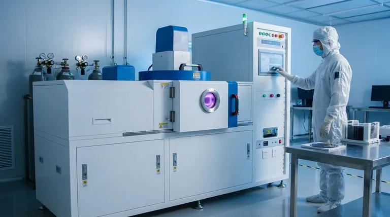
Creating a uniform, defect-free film that is only a few atoms thick requires highly specialized and often expensive equipment. The process is sensitive to contamination and requires precise control over temperature, pressure, and other variables.
Adhesion and Substrate Compatibility
A thin film is only as effective as its bond to the substrate beneath it. Poor adhesion is a primary mode of failure. Not all film materials stick well to all substrates, requiring careful selection or the use of intermediate bonding layers.
Inherent Fragility
While a film can add properties like hardness, the film itself can be fragile. A single scratch or microscopic defect can compromise the integrity of the entire layer, potentially exposing the substrate to corrosion or wear.
How to Leverage Thin Films for Your Goal
Choosing the right thin film strategy depends entirely on the problem you need to solve. Your desired outcome dictates the material, thickness, and deposition method.
- If your primary focus is durability and protection: Prioritize films known for hardness and chemical inertness, like titanium nitride or diamond-like carbon, to resist wear and corrosion.
- If your primary focus is optical performance: Focus on materials and layer thicknesses that precisely control the reflection, transmission, or absorption of specific light wavelengths.
- If your primary focus is electrical functionality: Select semiconductor or conductive materials and deposition methods that ensure the required purity and structural integrity for reliable performance.
- If your primary focus is cost-effective enhancement: Consider simpler decorative or reflective films that can be applied with less complex processes to improve aesthetics or basic functionality.
By understanding that thin films grant you control over a material's surface, you can unlock solutions to challenges that the bulk material alone could never address.
Summary Table:
| Application Category | Key Benefit | Common Examples |
|---|---|---|
| Mechanical & Chemical Protection | Wear and corrosion resistance | Cutting tools, aerospace components |
| Optical Manipulation | Precise light control | Anti-reflective coatings, thermal insulation glass |
| Electrical & Semiconductor | Enables modern electronics | Transistors, solar cells, memory storage |
Ready to enhance your materials with advanced thin film technology? KINTEK specializes in high-performance lab equipment and consumables for precise thin film deposition. Whether you need to improve durability, optical properties, or electronic functionality, our solutions are tailored to meet your specific laboratory needs. Contact us today to discuss how we can support your innovation!
Visual Guide
Related Products
- Aluminized Ceramic Evaporation Boat for Thin Film Deposition
- Tungsten Evaporation Boat for Thin Film Deposition
- Electron Beam Evaporation Coating Oxygen-Free Copper Crucible and Evaporation Boat
- Aluminum-Plastic Flexible Packaging Film for Lithium Battery Packaging
- Thin-Layer Spectral Electrolysis Electrochemical Cell
People Also Ask
- What is the widely used boat made of in thermal evaporation? Choosing the Right Material for High-Purity Deposition
- What is the source of evaporation for thin film? Choosing Between Thermal and E-Beam Methods
- What are the applications of thin films deposition? Unlock New Possibilities for Your Materials
- What is thin film deposition? Unlock Advanced Surface Engineering for Your Materials
- Why is an alumina boat selected for catalyst precursors? Ensure Sample Purity at 1000 °C


