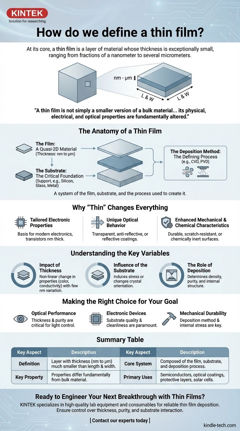
At its core, a thin film is a layer of material whose thickness is exceptionally small, ranging from fractions of a nanometer to several micrometers. This layer is deposited onto a surface, known as a substrate, and is defined by the fact that its thickness is orders of magnitude smaller than its length and width. This dramatic reduction in one dimension is what gives thin films their unique and powerful properties.
The critical concept to grasp is that a thin film is not simply a smaller version of a bulk material. By suppressing its third dimension to the nano or micro scale, its physical, electrical, and optical properties are fundamentally altered, enabling technologies that would otherwise be impossible.
The Anatomy of a Thin Film
To truly understand a thin film, one must consider it not as a standalone object, but as a system composed of three integral parts: the film itself, the substrate it rests on, and the process used to create it.
The Film: A Quasi-2D Material
A thin film is often described as a 2-dimensional material. While it still possesses thickness, this dimension is so constrained that surface effects begin to dominate its behavior over the bulk, volume-based properties we experience in everyday objects.
The specific thickness is dictated entirely by the intended application, from a single layer of atoms (a monolayer) to more robust, multi-micrometer coatings.
The Substrate: The Critical Foundation
The film is almost always deposited onto a substrate, such as silicon, glass, or metal. The substrate provides the necessary mechanical support.
Crucially, the properties of the substrate—its crystal structure, smoothness, and material composition—can significantly influence the final characteristics of the film grown upon it.
The Deposition Method: The Defining Process
A film's properties are inseparable from how it was made. The deposition technique is a key variable that determines the film's density, purity, and internal structure.
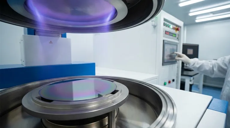
Common methods include Chemical Vapor Deposition (CVD), which uses precursor gases to form coatings, and Physical Vapor Deposition (PVD), which involves evaporating or sputtering material onto the substrate.
Why "Thin" Changes Everything
The technological value of a thin film comes directly from the unique phenomena that occur at this incredibly small scale. These properties are rarely observed in the material's bulk form.
Tailored Electronic Properties
In materials like semiconducting silicon, constraining the material into a thin film is the basis for modern electronics. It allows for the creation of transistors and complex circuits that are nanometers thick.
Unique Optical Behavior
Thin film coatings can be engineered to be transparent, anti-reflective, or highly reflective. This precision control over light is essential for lenses, solar cells, and display screens.
Enhanced Mechanical and Chemical Characteristics
Thin films can create surfaces that are exceptionally durable, scratch-resistant, or chemically inert. These coatings protect everything from medical implants to industrial drill bits.
Understanding the Key Variables
The performance of a thin film is not absolute; it is a direct result of carefully controlled variables. Misunderstanding these factors is the primary source of failure in thin film applications.
Impact of Thickness
A change of even a few nanometers in thickness can dramatically alter a film's color, electrical conductivity, or transparency. This is not a linear relationship; properties can change in complex ways as thickness varies.
Influence of the Substrate
Depositing the same film on glass versus a silicon wafer can yield two entirely different outcomes. The substrate can induce stress or influence the crystal orientation of the film, changing its performance.
The Role of Deposition
A film deposited via PVD may be denser and under more stress than an identical film grown with CVD. The choice of deposition technology is a fundamental engineering decision based on the required properties and cost.
Making the Right Choice for Your Goal
The definition of an "optimal" thin film is entirely dependent on its purpose. Consider your primary objective when specifying or designing a thin film component.
- If your primary focus is optical performance: Thickness and material purity are your most critical variables, as they directly control light transmission and reflection.
- If your primary focus is electronic devices: The quality of the substrate and the cleanliness of the deposition process are paramount to creating reliable semiconductor circuits.
- If your primary focus is mechanical durability: The deposition method and internal stress of the film are key factors in creating a hard, resilient coating.
Ultimately, a thin film is a highly engineered material layer where small scale enables unprecedented control over its fundamental properties.
Summary Table:
| Key Aspect | Description |
|---|---|
| Definition | A layer of material with a thickness (nm to µm) much smaller than its length and width. |
| Core System | Composed of the film itself, the substrate it's on, and the deposition process used. |
| Key Property | Properties (electrical, optical, mechanical) differ fundamentally from the bulk material. |
| Primary Uses | Semiconductors, optical coatings, protective layers, and solar cells. |
Ready to Engineer Your Next Breakthrough with Thin Films?
The precise application of thin films is critical to the success of your R&D and manufacturing processes. KINTEK specializes in providing the high-quality lab equipment and consumables necessary for reliable thin film deposition, from research to production.
Our expertise ensures you have the right tools to control thickness, purity, and substrate interaction—key variables for achieving the desired electronic, optical, or mechanical properties in your application.
Let's discuss your specific needs. Contact our experts today to find the perfect solution for your laboratory.
Visual Guide
Related Products
- Aluminized Ceramic Evaporation Boat for Thin Film Deposition
- Tungsten Evaporation Boat for Thin Film Deposition
- Electron Beam Evaporation Coating Oxygen-Free Copper Crucible and Evaporation Boat
- Molybdenum Tungsten Tantalum Evaporation Boat for High Temperature Applications
- Aluminum-Plastic Flexible Packaging Film for Lithium Battery Packaging
People Also Ask
- What are the applications of thin films deposition? Unlock New Possibilities for Your Materials
- What is the widely used boat made of in thermal evaporation? Choosing the Right Material for High-Purity Deposition
- What is the chemical method for thin film deposition? Build Films from the Molecular Level Up
- Why are high-purity ceramic boats used for lignin activation? Ensure Purity & Thermal Stability
- What are thin films deposited by evaporation? A Guide to High-Purity Coating


