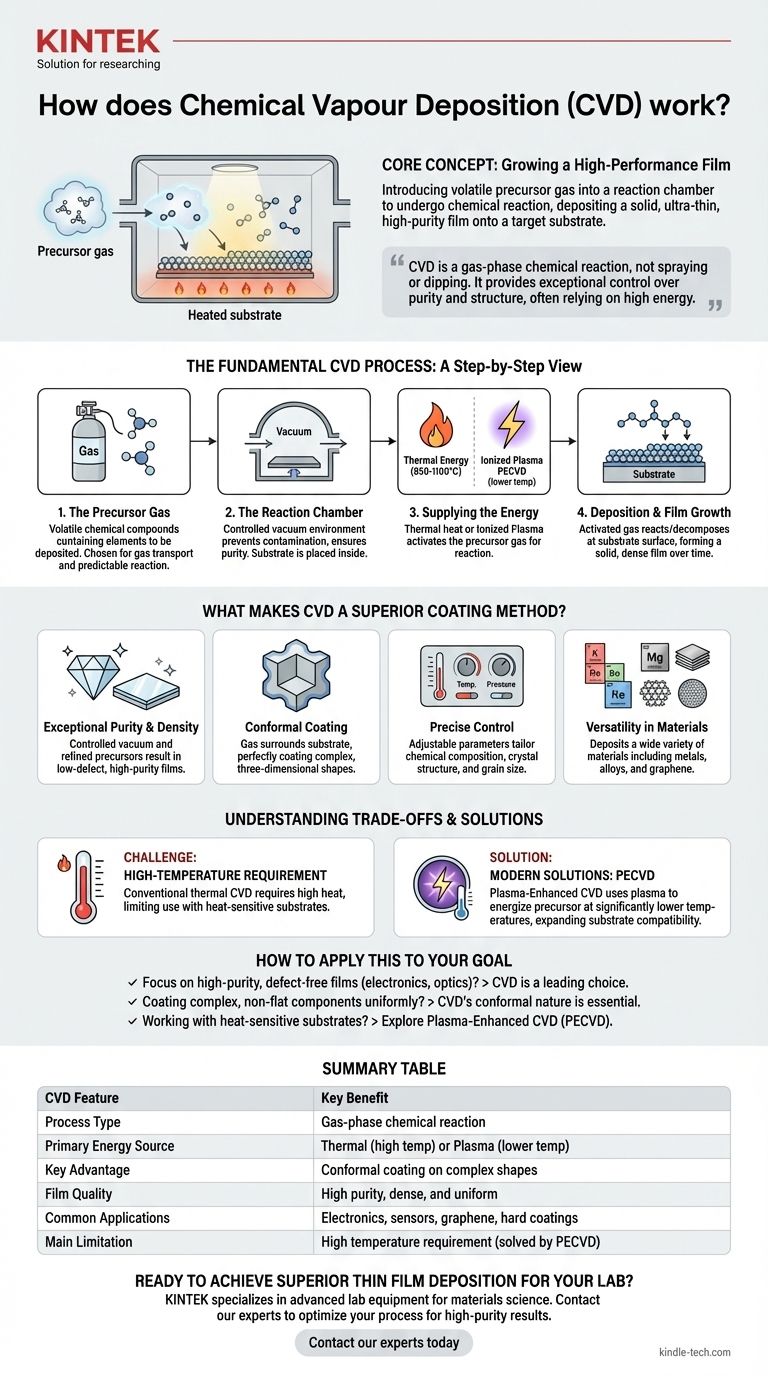
At its core, Chemical Vapor Deposition (CVD) is a sophisticated process for "growing" an ultra-thin, high-performance film onto a surface. It works by introducing a volatile precursor gas into a reaction chamber. When energy is applied, this gas undergoes a chemical reaction or decomposition, depositing a solid layer onto the target material, known as the substrate. This process builds the desired film molecule by molecule.
Chemical Vapor Deposition is not a simple spraying or dipping process; it is a gas-phase chemical reaction that builds a solid film directly onto a substrate. This method provides exceptional control over a film's purity and structure, but its reliance on high energy—often intense heat—is its most significant trade-off.
The Fundamental CVD Process: A Step-by-Step View
To truly understand CVD, it's best to break it down into its core operational stages. Each step is critical for achieving a high-quality, uniform final product.
The Precursor Gas
The process begins with one or more volatile precursor gases. These are chemical compounds that contain the elements you want to deposit. They are chosen specifically for their ability to be transported as a gas and to react predictably under certain conditions.
The Reaction Chamber
The precursor gas is injected into a sealed chamber, which typically operates under a vacuum. This controlled environment is crucial for preventing contamination from air and ensuring the purity of the deposited film. The component to be coated—the substrate—is placed inside this chamber.
Supplying the Energy
For the chemical reaction to occur, energy must be supplied. There are two primary methods for this.
The most common is thermal energy, where the substrate is heated to a high reaction temperature (often 850-1100°C). This intense heat provides the energy needed to break down the precursor gas.
Alternatively, an ionized plasma can be used. Methods like Plasma-Enhanced CVD (PECVD) use electromagnetic fields to create a plasma, which activates the precursor gas at much lower temperatures.
The Deposition and Film Growth
Once activated by the energy source, the precursor gas reacts or decomposes at or near the substrate surface. This chemical change leaves behind a solid material that bonds directly to the substrate, forming a thin, dense film.
Over time, this deposition process continues, building up the film to the desired thickness in a highly controlled and uniform manner.
What Makes CVD a Superior Coating Method?
The reason CVD is a leading approach for manufacturing advanced materials like graphene is due to a unique set of advantages that stem directly from its gas-phase deposition mechanism.
Exceptional Purity and Density
Because the process occurs in a controlled vacuum environment with highly refined precursor gases, the resulting films have extremely high purity and good denseness. This low-defect quality is essential for applications like high-performance electronics and sensors.
Conformal Coating for Complex Shapes
Unlike line-of-sight deposition methods (like spraying), the precursor gas in CVD surrounds the substrate entirely. This results in a perfectly conformal coating that uniformly covers complex, three-dimensional shapes, a characteristic often described as a "good wrap-around property."
Precise Control Over Material Properties
By carefully adjusting parameters like temperature, pressure, and gas composition, engineers can precisely control the final film's characteristics. This includes its chemical composition, crystal structure, and even grain size, allowing for highly tailored materials.
Versatility in Materials
CVD is an incredibly versatile technique. It can be used to deposit a wide variety of materials, including metal films, non-metal films like graphene, multi-component alloys, and hard ceramic layers.
Understanding the Trade-offs and Limitations
No technical process is without its challenges. The primary limitation of traditional CVD is directly linked to its greatest strength: the use of high energy.
The High-Temperature Requirement
Conventional thermal CVD requires extremely high temperatures to initiate the chemical reaction. Many potential substrate materials simply cannot withstand this heat without melting, warping, or degrading, which severely limits the range of possible applications.
Modern Solutions: Plasma-Enhanced CVD (PECVD)
To overcome the temperature limitation, methods like Plasma-Enhanced CVD (PECVD) were developed. By using plasma instead of heat to energize the precursor gas, deposition can occur at significantly lower temperatures, making the process compatible with a much wider array of substrates.
Substrate Compatibility
Even with lower-temperature options, substrate compatibility remains a key consideration. The substrate's surface chemistry and physical properties must allow for the strong bonding of the deposited film.
How to Apply This to Your Goal
Choosing a deposition method depends entirely on the specific requirements of your material and application.
- If your primary focus is creating high-purity, defect-free thin films for electronics or optics: CVD is a leading choice due to its precise control over film structure and composition.
- If your primary focus is coating complex, non-flat components uniformly: CVD's conformal nature ensures an even layer across the entire surface where other methods would fail.
- If you are working with heat-sensitive substrates like polymers or certain alloys: You must look beyond traditional thermal CVD and explore lower-temperature variants like Plasma-Enhanced CVD (PECVD).
Ultimately, understanding the principles of CVD empowers you to select the right material deposition strategy for the most demanding applications.
Summary Table:
| CVD Feature | Key Benefit |
|---|---|
| Process Type | Gas-phase chemical reaction |
| Primary Energy Source | Thermal (high temp) or Plasma (lower temp) |
| Key Advantage | Conformal coating on complex shapes |
| Film Quality | High purity, dense, and uniform |
| Common Applications | Electronics, sensors, graphene, hard coatings |
| Main Limitation | High temperature requirement (solved by PECVD) |
Ready to achieve superior thin film deposition for your lab?
KINTEK specializes in providing advanced lab equipment and consumables for materials science and research. Whether you are developing next-generation electronics, coating complex components, or exploring nanomaterials like graphene, our expertise in deposition technologies can help you optimize your process for high-purity, uniform results.
Contact our experts today to discuss how our solutions can enhance your research and development capabilities.
Visual Guide
Related Products
- CVD Diamond Dressing Tools for Precision Applications
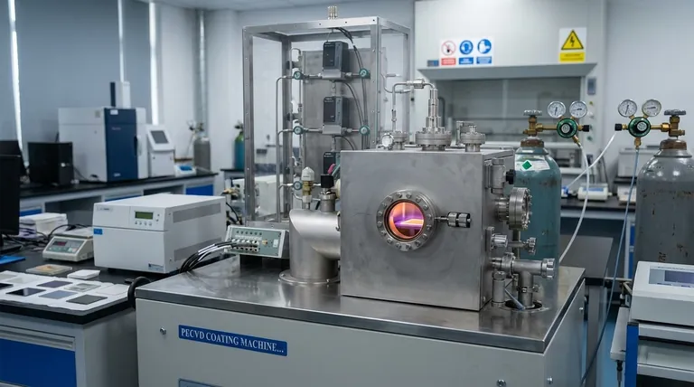
- Multi Heating Zones CVD Tube Furnace Machine Chemical Vapor Deposition Chamber System Equipment
- CVD Diamond Domes for Industrial and Scientific Applications
- CVD Diamond for Thermal Management Applications
- Chemical Vapor Deposition CVD Equipment System Chamber Slide PECVD Tube Furnace with Liquid Gasifier PECVD Machine
People Also Ask
- What are the disadvantages of CVD diamonds? Understanding the trade-offs for your purchase.
- What color diamonds are CVD? Understanding the Process from Brown Tint to Colorless Beauty
- How do you identify a CVD diamond? The Definitive Guide to Lab-Grown Diamond Verification
- What are the raw materials for CVD diamonds? A seed, a gas, and the science of crystal growth.
- How long does it take to make synthetic diamonds? Discover the 6-8 Week Science Behind Lab-Grown Gems


