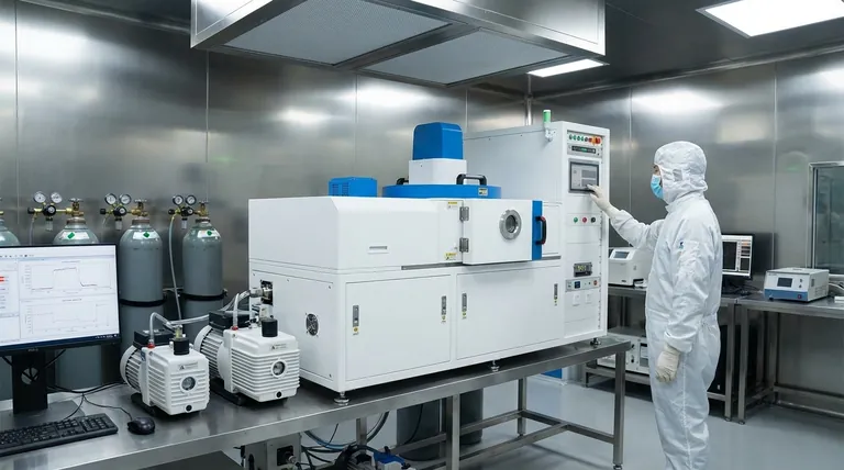
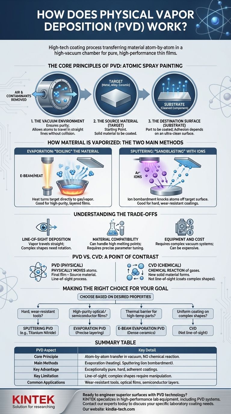
At its core, physical vapor deposition (PVD) is a high-tech coating process that transfers a material atom-by-atom from a solid source onto a target surface. This is all done within a high-vacuum chamber. The process involves three fundamental steps: a source material is converted into a vapor, this vapor travels across the vacuum, and it finally condenses onto the substrate as a thin, highly adherent film.
Physical Vapor Deposition should be understood not as a single method, but as a family of "line-of-sight" vacuum deposition techniques. The core principle is physically moving a material from a source to a target without chemical reactions, enabling the creation of exceptionally pure and high-performance thin films.
The Core Principles of PVD
To understand how PVD works, it's best to think of it as a highly controlled form of atomic spray painting. The process relies on three key components: the vacuum environment, the source material (target), and the destination surface (substrate).
The Vacuum Environment
The entire PVD process takes place in a vacuum chamber. This is non-negotiable for two reasons.
First, the vacuum removes air and other gas molecules that could react with or contaminate the vaporized material, ensuring the purity of the final film.
Second, in an empty space, the vaporized atoms can travel in a straight line from the source to the substrate without colliding with air molecules, which would otherwise scatter them.
The Source Material ("Target")
This is the solid material—often a metal, alloy, or ceramic—that will become the coating. It is placed inside the vacuum chamber and is the starting point of the process.
The Destination Surface ("Substrate")
This is the part or component that is to be coated. Substrates are cleaned meticulously before being placed in the chamber, as the quality of the film's adhesion depends on an ultra-clean surface.
How Material is Vaporized: The Two Main Methods
The "physical" part of PVD refers to the mechanism used to turn the solid target material into a vapor. This is achieved not through chemical reactions, but through the application of physical energy. The two dominant methods are evaporation and sputtering.
Evaporation: "Boiling" the Material
In this method, the target material is heated in the vacuum until it evaporates or sublimes, turning directly into a gas.
This heating is often accomplished using a high-energy electron beam (e-beam evaporation) that can bring even materials with very high melting points to a vapor phase. The resulting vapor then travels and condenses on the cooler substrate.
Sputtering: "Sandblasting" with Ions
Sputtering is a fundamentally different process. Instead of being boiled off, atoms are knocked off the target's surface.
This is done by introducing an inert gas (like Argon) into the chamber and applying a high voltage. This creates a plasma, and the gas ions are accelerated into the target, striking it with enough force to eject, or "sputter," individual atoms. These ejected atoms then travel to the substrate and deposit as a film.
Understanding the Trade-offs
While powerful, PVD is not a universal solution. Understanding its inherent limitations is key to using it effectively.
Line-of-Sight Deposition
Because the vaporized atoms travel in a straight line, PVD is a line-of-sight process. Surfaces that are hidden or in deep cavities will not get coated evenly unless the substrate is rotated or repositioned during the process.
Material Compatibility
While PVD can handle a wide range of materials, including those with high melting points, the specific parameters must be carefully tuned for each one. Creating alloys or complex compound films requires multiple sources and precise control.
Equipment and Cost
PVD systems require high-vacuum pumps, high-voltage power supplies, and sophisticated control systems. This makes the equipment complex and expensive, often placing it out of reach for small-scale operations.
A Point of Contrast: PVD vs. CVD
To further clarify what PVD is, it helps to compare it to the other major deposition technique: Chemical Vapor Deposition (CVD).
The Core Difference: Physical vs. Chemical
The name says it all. PVD physically moves atoms from a source to a target. The material of the final film is the same as the source material.
CVD, on the other hand, introduces precursor gases into a chamber. A chemical reaction is then triggered on the substrate's surface, creating a new solid material that forms the coating. Because it relies on gas, CVD is not a line-of-sight process and can coat complex shapes more uniformly.
Making the Right Choice for Your Goal
Selecting a coating technology depends entirely on the desired properties of the final product.
- If your primary focus is a hard, wear-resistant coating for tools: Sputtering PVD is an excellent choice for applying materials like titanium nitride.
- If your primary focus is a high-purity optical film for lenses or semiconductors: Evaporation PVD provides the control needed for precise layering and purity.
- If your primary focus is a thermal barrier for a high-temperature part (e.g., aerospace): E-beam evaporation PVD can deposit dense, temperature-resistant ceramic coatings.
- If your primary focus is uniformly coating a complex internal geometry: CVD is often a more suitable choice than the line-of-sight PVD process.
By understanding its principles and trade-offs, you can leverage PVD to create materials with precisely engineered surfaces.
Summary Table:
| PVD Aspect | Key Detail |
|---|---|
| Core Principle | Atom-by-atom transfer of material in a vacuum, without chemical reactions. |
| Main Methods | Evaporation (heating) and Sputtering (ion bombardment). |
| Key Advantage | Creates exceptionally pure, hard, and adherent coatings. |
| Key Limitation | Line-of-sight process; complex shapes require part manipulation. |
| Common Applications | Wear-resistant tool coatings, optical films, semiconductor layers. |
Ready to engineer superior surfaces with PVD technology?
KINTEK specializes in high-performance lab equipment, including PVD systems for creating durable, pure thin films. Whether you're developing advanced optics, wear-resistant tools, or semiconductor components, our expertise can help you achieve precise and reliable results.
Contact our experts today to discuss how a PVD solution from KINTEK can meet your specific laboratory coating needs.
Visual Guide
Related Products
- Chemical Vapor Deposition CVD Equipment System Chamber Slide PECVD Tube Furnace with Liquid Gasifier PECVD Machine
- RF PECVD System Radio Frequency Plasma-Enhanced Chemical Vapor Deposition RF PECVD
- Customer Made Versatile CVD Tube Furnace Chemical Vapor Deposition Chamber System Equipment
- Microwave Plasma Chemical Vapor Deposition MPCVD Machine System Reactor for Lab and Diamond Growth
- Custom CVD Diamond Coating for Lab Applications
People Also Ask
- What is plasma enhanced chemical vapor deposition PECVD equipment? A Guide to Low-Temperature Thin Film Deposition
- What is the chemical vapor deposition growth process? Build Superior Thin Films from the Atom Up
- What are the core advantages of PE-CVD in OLED encapsulation? Protect Sensitive Layers with Low-Temp Film Deposition
- What are the advantages of chemical vapor deposition? Achieve Superior Thin Films for Your Lab
- How expensive is chemical vapor deposition? Understanding the True Cost of High-Performance Coating


