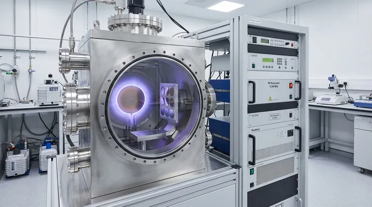
At its core, RF magnetron sputtering is a sophisticated vacuum deposition technique used to create ultra-thin films. It works by generating a plasma from an inert gas, like argon, using a radio frequency (RF) electric field. Strong magnets confine this plasma near a source material, called a target, causing energized argon ions to bombard it and eject atoms, which then coat a nearby object, or substrate.
The crucial insight is that RF sputtering solves a fundamental problem: the inability of simpler DC sputtering to deposit non-conductive materials. By rapidly alternating the electric field, it prevents a charge buildup on insulating targets, making it a uniquely versatile tool for creating advanced coatings from virtually any material.
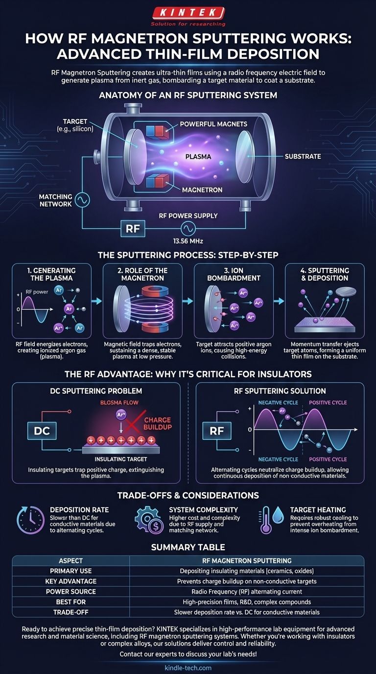
The Anatomy of an RF Sputtering System
To understand the process, we must first understand the key components working together inside a high-vacuum chamber. This controlled environment is critical to prevent contamination and allow the sputtered atoms to travel freely.
The Target and Substrate
The target is a disc or ingot made of the material you wish to deposit as a thin film. The substrate is the object you are coating, such as a silicon wafer, glass slide, or medical implant.
The Inert Gas
An inert gas, almost always argon, is introduced into the chamber at a very low pressure. This gas does not react with the target material; its sole purpose is to be ionized to create the plasma that drives the process.
The RF Power Supply
Instead of a constant negative voltage (DC), an RF power supply applies a high-frequency alternating voltage (commonly 13.56 MHz) to the target. This alternating field is the key to the entire process.
The Magnetron
A set of powerful permanent magnets is placed behind the target. This assembly is the "magnetron" part of the name, and its magnetic field plays a critical role in improving the system's efficiency.
The Sputtering Process, Step-by-Step
These components work in a precise sequence to build a film one atom at a time.
Step 1: Generating the Plasma
The RF power supply oscillates the electric field, energizing free electrons within the low-pressure argon gas. These high-energy electrons collide with neutral argon atoms, knocking off their electrons and creating a cloud of positively charged argon ions (Ar+) and more free electrons. This ionized gas is the plasma.
Step 2: The Role of the Magnetron
The magnetic field from the magnetron traps the highly mobile electrons, forcing them into a spiral path directly in front of the target's surface. This greatly increases the probability that an electron will collide with and ionize an argon atom, sustaining a dense, stable plasma even at very low pressures.
Step 3: Ion Bombardment
The target acts as a cathode. During the negative portion of the RF cycle, it develops a strong negative bias, attracting the positively charged argon ions from the plasma. These ions accelerate and slam into the target surface with immense kinetic energy.
Step 4: Sputtering and Deposition
If the energy of the bombarding ion is high enough, it transfers its momentum to the target's atoms, ejecting them into the vacuum chamber. This ejection process is sputtering. These sputtered atoms travel in a straight line until they strike the substrate, gradually building up to form a uniform thin film.
Why Radio Frequency is the Critical Component
The use of RF power is not an arbitrary choice; it is a direct solution to a major limitation of simpler sputtering methods.
The Problem with Sputtering Insulators
If you try to sputter an insulating (dielectric) material like a ceramic or oxide using a direct current (DC) power supply, the process quickly fails. The bombardment of positive argon ions cannot be neutralized by the non-conductive target, causing a positive charge to build up on its surface. This "surface charging" eventually repels any more incoming argon ions, extinguishing the plasma and stopping the process entirely.
The RF Solution: Alternating Cycles
The RF power supply brilliantly solves this by alternating the target's voltage millions of times per second.
- Negative Cycle: The target is negatively biased, attracting argon ions for sputtering, just as described above. This is the productive part of the cycle.
- Positive Cycle: For a brief moment, the target becomes positively biased. It now attracts the highly mobile electrons from the plasma, which effectively neutralize the positive charge built up during the previous cycle.
This rapid oscillation cleanses the target of charge, allowing the sputtering of insulating materials to proceed continuously.
Understanding the Trade-offs
While powerful, RF magnetron sputtering is not always the optimal choice. It involves clear trade-offs in performance and complexity.
Deposition Rate
For conductive materials like pure metals, RF sputtering is generally slower than its DC magnetron sputtering counterpart. The short positive cycle, while necessary for insulators, represents a brief pause in productive sputtering.
System Complexity and Cost
RF systems are inherently more complex. They require an expensive RF power supply and an impedance matching network to efficiently transfer power to the plasma. This makes them more costly to purchase and maintain than DC systems.
Target Heating
The intense ion bombardment generates a significant amount of heat on the target. This requires robust water cooling systems to prevent the target from overheating, melting, or cracking, especially for materials with low thermal conductivity.
Making the Right Choice for Your Goal
Selecting the correct sputtering technique depends entirely on the material you are depositing and your project's priorities.
- If your primary focus is depositing a conductive material (like a pure metal): DC magnetron sputtering is often faster, simpler, and more cost-effective.
- If your primary focus is depositing an insulating material (like a ceramic, oxide, or nitride): RF magnetron sputtering is the essential and correct choice to overcome the issue of surface charging.
- If your primary focus is depositing complex alloys or compounds with high precision: RF sputtering provides excellent control over film quality and composition, making it a preferred method for advanced research and development.
By understanding these core principles, you can confidently select the precise tool needed to engineer advanced thin-film materials.
Summary Table:
| Aspect | RF Magnetron Sputtering |
|---|---|
| Primary Use | Depositing insulating materials (ceramics, oxides) |
| Key Advantage | Prevents charge buildup on non-conductive targets |
| Power Source | Radio Frequency (RF) alternating current |
| Best For | High-precision films, R&D, complex compounds |
| Trade-off | Slower deposition rate vs. DC for conductive materials |
Ready to achieve precise thin-film deposition in your lab? KINTEK specializes in high-performance lab equipment, including RF magnetron sputtering systems designed for advanced research and material science. Whether you're working with insulating ceramics, complex alloys, or need superior film quality, our solutions deliver the control and reliability your projects demand. Contact our experts today to discuss how we can support your laboratory's specific needs!
Visual Guide
Related Products
People Also Ask
- What is plasma enhanced chemical Vapour deposition process used for fabrication of? A Guide to Low-Temperature Thin Films
- What is the role of RF-PECVD in VFG preparation? Mastering Vertical Growth and Surface Functionality
- What is plasma enhanced chemical vapour deposition process? Unlock Low-Temperature, High-Quality Thin Films
- What is plasma CVD? Unlock Low-Temperature Thin Film Deposition for Sensitive Materials
- What is plasma enhanced chemical vapour deposition PECVD used for? Enable Low-Temp Thin Films for Electronics & Solar
