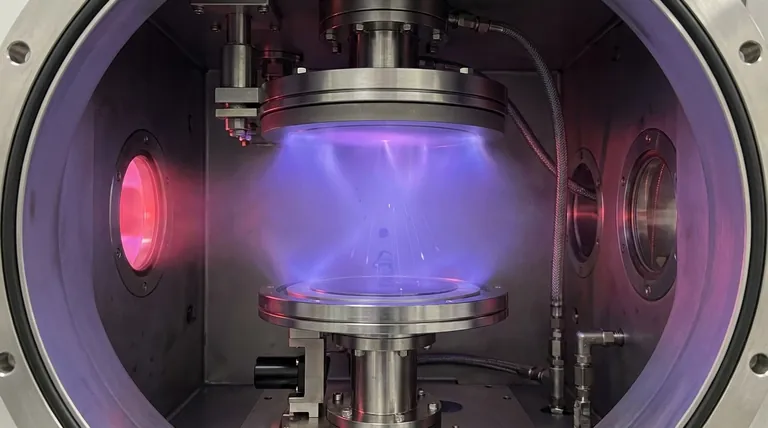
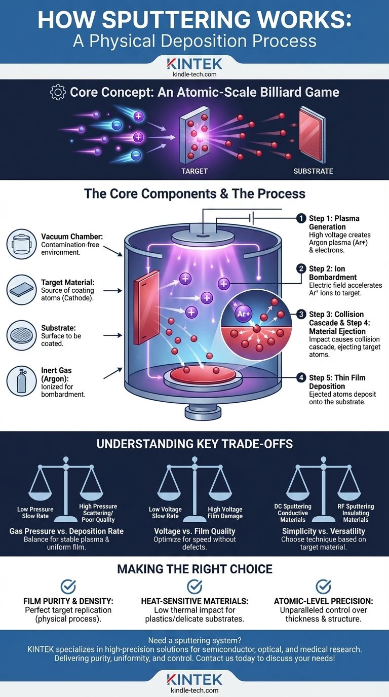
At its core, sputtering is a physical deposition process used to apply an exceptionally thin and uniform coating of one material onto another. It works by creating a plasma in a vacuum and using the resulting ions as microscopic projectiles. These ions bombard a "target" made of the coating material, physically knocking atoms loose, which then travel and deposit onto the "substrate," forming the desired film.
Sputtering is best understood not as a chemical or thermal process, but as a highly controlled mechanical one. It is an atomic-scale billiard game, where high-energy gas ions are used to precisely chip away atoms from a source material and redeposit them onto a surface.
The Core Components of a Sputtering System
To understand the process, you must first understand the environment where it takes place. Every sputtering system is built around four key components working in concert.
The Vacuum Chamber
The entire process occurs inside a sealed chamber from which nearly all air has been removed. This vacuum is critical because it prevents atoms from the air (like oxygen or nitrogen) from contaminating the film and ensures the sputtered atoms can travel freely from the target to the substrate without colliding with other particles.
The Target Material
This is a block or plate made of the material you want to create the film from, such as titanium, gold, or silicon dioxide. A high negative voltage is applied to the target, making it a cathode.
The Substrate
This is the object you intend to coat, such as a silicon wafer, a piece of glass, or a medical implant. The substrate is positioned to face the target and acts as the collection surface for the sputtered atoms.
The Inert Sputtering Gas
A small, precisely controlled amount of an inert gas, most commonly Argon (Ar), is introduced into the vacuum chamber. This gas is not part of the final coating; its sole purpose is to be ionized and serve as the bombardment particles.
The Physics of the Process: From Plasma to Film
With the components in place, the sputtering process unfolds in a rapid, precisely controlled sequence of physical events.
Step 1: Plasma Generation
When the high voltage is applied to the target, it creates a powerful electric field within the low-pressure Argon gas. This field energizes free electrons, causing them to collide with Argon atoms and knock off other electrons. This creates a cascade effect, resulting in a stable, glowing plasma—a cloud of positively charged Argon ions (Ar+) and free electrons.
Step 2: Ion Bombardment
The positively charged Argon ions (Ar+) are strongly attracted to the negatively charged target (the cathode). The electric field accelerates these ions, causing them to slam into the surface of the target at very high velocity.
Step 3: The Collision Cascade
A single ion impact is far more complex than just chipping off a surface atom. The high-energy ion penetrates the first few atomic layers of the target, transferring its momentum and setting off a collision cascade—a chain reaction of atom-on-atom collisions beneath the surface.
Step 4: Material Ejection
When this cascade of kinetic energy works its way back to the target's surface, it can give a surface atom enough energy to overcome its atomic binding energy. This is the force holding it to the other atoms. Once that threshold is crossed, the atom is ejected, or "sputtered," into the vacuum chamber.
Step 5: Thin Film Deposition
These newly freed atoms from the target travel in a general line-of-sight path through the vacuum chamber. When they strike the substrate, they condense on its surface. Over time, millions of these arriving atoms build up, layer by layer, to form a dense, uniform, and highly pure thin film.
Understanding the Key Trade-offs
Sputtering offers incredible control, but its effectiveness depends on a careful balance of process variables. Understanding these trade-offs is key to achieving a successful outcome.
Gas Pressure vs. Deposition Rate
The pressure of the sputtering gas inside the chamber is a critical parameter. If the pressure is too low, there won't be enough gas ions to generate a stable plasma, leading to a very slow sputtering rate. If the pressure is too high, the atoms ejected from the target are more likely to collide with gas atoms on their way to the substrate, scattering them and reducing the quality and uniformity of the film.
Voltage vs. Film Quality
Increasing the voltage accelerates the ions with more energy, which typically increases the rate of sputtering. However, excessively high energy can damage the delicate structure of the growing film or even the substrate itself, introducing defects. The optimal voltage is a balance between a practical deposition speed and the desired film properties.
Simplicity vs. Versatility
The basic sputtering process described here (DC sputtering) works exceptionally well for electrically conductive target materials. However, it fails for insulating (dielectric) materials. To sputter insulators, a more complex technique called RF (Radio Frequency) sputtering is required, which involves alternating the electric field to overcome charge buildup.
Making the Right Choice for Your Goal
Understanding the mechanics of sputtering allows you to recognize when and why it is the superior choice for thin-film deposition.
- If your primary focus is film purity and density: Sputtering is ideal because it's a physical momentum-transfer process, not a chemical or high-heat evaporation process, resulting in films that perfectly replicate the target's composition.
- If your primary focus is coating heat-sensitive materials: Because sputtering is not primarily a thermal process, it can deposit high-performance films onto plastics and other materials that would be damaged by traditional high-temperature methods.
- If your primary focus is atomic-level precision: The atom-by-atom nature of sputtering provides unparalleled control over film thickness, uniformity, and structure, which is critical for advanced optics, semiconductors, and electronics.
By viewing sputtering as a process of controlled atomic bombardment, you can effectively leverage its unique capabilities to engineer materials with exacting specifications.
Summary Table:
| Key Component | Role in the Sputtering Process |
|---|---|
| Vacuum Chamber | Provides a contamination-free environment for atom travel |
| Target Material | Source of coating atoms, negatively charged (cathode) |
| Substrate | Surface to be coated (e.g., silicon wafer, glass) |
| Inert Gas (Argon) | Ionized to form plasma and bombard the target |
| High Voltage | Accelerates ions to eject target atoms via collision cascade |
Need a sputtering system for your lab's thin-film research? KINTEK specializes in high-precision lab equipment, including sputtering systems for semiconductor, optical, and medical coating applications. Our solutions deliver the purity, uniformity, and control your projects demand. Contact us today to discuss your specific needs!
Visual Guide
Related Products
- Spark Plasma Sintering Furnace SPS Furnace
- Vacuum Induction Melting Spinning System Arc Melting Furnace
- Chemical Vapor Deposition CVD Equipment System Chamber Slide PECVD Tube Furnace with Liquid Gasifier PECVD Machine
- Customer Made Versatile CVD Tube Furnace Chemical Vapor Deposition Chamber System Equipment
People Also Ask
- What is the mechanism of SPS process? A Deep Dive into Rapid, Low-Temperature Sintering
- What technical advantages does a Spark Plasma Sintering (SPS) furnace offer for LZP ceramics? Enhance Ionic Conductivity
- What is the process fundamentals of spark plasma sintering? Achieve Rapid, High-Density Material Consolidation
- What is the theory of spark plasma sintering? A Guide to Rapid, Low-Temperature Densification
- Why are Spark Plasma Sintering (SPS) furnaces or hot presses utilized in the preparation of Li3PS4 solid electrolytes?


