At its core, thin film technology is the science of adding new capabilities to a material by applying an exceptionally thin layer—often just a few atoms or molecules thick—to its surface. This process grants advantages like electrical conductivity, corrosion resistance, and specific optical properties, making it foundational to industries ranging from modern electronics and renewable energy to simple decorative coatings.
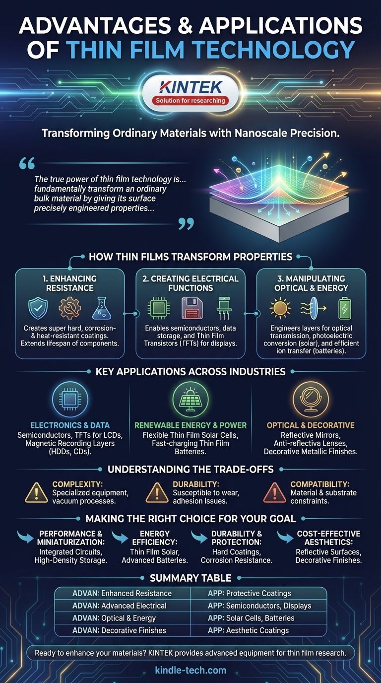
The true power of thin film technology is not in the film itself, but in its ability to fundamentally transform an ordinary bulk material by giving its surface precisely engineered properties that it does not naturally possess.
How Thin Films Transform Material Properties
Thin film deposition allows us to bestow ideal surface characteristics onto a cost-effective or structurally sound base material, known as a substrate. This creates a composite with the best properties of both.
Enhancing Mechanical and Chemical Resistance
A primary advantage is protection. By depositing a specialized layer, we can make an underlying material far more durable.
This includes creating super hard, corrosion-resistant, heat-resistant, and oxidation-resistant films. These protective coatings dramatically extend the lifespan and performance of mechanical components and tools.
Creating Advanced Electrical Functions
Thin films are the bedrock of modern electronics. They enable the creation of microscopic circuits and components on substrates like silicon wafers.
Functional films are designed for tasks like magnetic recording, information storage, and creating semiconductors. This is the basis for computer chips, disk drives, and the thin film transistors (TFTs) vital for high-quality displays.
Manipulating Optical and Energy Properties
Thin films can be engineered to interact with light and energy in highly specific ways.
This includes creating layers for optical transmission in displays, photoelectric conversion in solar cells, and efficient ion transfer in batteries. These capabilities are essential for developing next-generation energy and optical devices.
Key Applications Across Industries
The ability to precisely modify a surface has unlocked revolutionary applications in nearly every technological field.
In Modern Electronics and Data Storage
The miniaturization and performance of electronics are directly tied to thin film technology.
It is integral to producing semiconductors, thin film transistors (TFTs) for liquid crystal displays (LCDs), and magnetic recording layers for hard drives and CDs. TFTs, for example, improve the response time and energy efficiency of modern screens.
In Renewable Energy and Power
Thin films are making energy generation and storage lighter, more flexible, and more efficient.
Thin film solar cells are significantly lighter than traditional silicon panels, making them suitable for applications like photovoltaic glazing on buildings. Thin film batteries charge faster, last longer, and have a higher energy density, improving everything from medical implants to grid-scale energy storage.
In Optical and Decorative Coatings
Some of the most common applications are also the simplest. Thin films are used to manipulate light or provide an aesthetic finish.
This includes the reflective layers in mirrors, anti-reflective coatings on lenses, and a vast range of decorative coatings that give inexpensive materials like plastic the appearance of metal.
Understanding the Trade-offs
While incredibly powerful, thin film technology is not without its challenges. The process of deposition and the nature of the films themselves present practical limitations.
The Complexity of Deposition
Applying a uniform film that is only nanometers thick requires highly specialized and expensive equipment.
Processes like sputtering occur in a vacuum and require precise control over temperature, pressure, and materials. This complexity can be a significant barrier to entry and cost.
Film Durability and Adhesion
A film is only as good as its bond to the substrate. Poor adhesion can cause the film to peel, flake, or delaminate, rendering the component useless.
Furthermore, because the films are so thin, they can be susceptible to scratches or wear, sometimes requiring an additional protective topcoat which adds complexity.
Material and Substrate Compatibility
Not every material can be deposited onto every substrate. Chemical, thermal, and structural incompatibilities can prevent the formation of a stable, functional film.
Extensive research and development are often required to find the right combination of film material, substrate, and deposition process for a specific application.
Making the Right Choice for Your Goal
Selecting the right thin film approach depends entirely on the problem you need to solve.
- If your primary focus is performance and miniaturization: Utilize thin films to create integrated circuits, thin film transistors, and high-density data storage.
- If your primary focus is energy efficiency and generation: Look to thin film solar cells for flexible designs and thin film batteries for faster-charging, longer-lasting power.
- If your primary focus is component durability and protection: Apply super hard, corrosion-resistant coatings to enhance the lifespan and resilience of mechanical parts or tools.
- If your primary focus is cost-effective aesthetics or optics: Employ thin film coatings for reflective surfaces like mirrors, anti-glare lenses, or decorative finishes.
Ultimately, thin film technology empowers you to choose the best bulk material for the job and then add the exact surface properties required for optimal performance.
Summary Table:
| Key Advantage | Primary Application |
|---|---|
| Enhanced Mechanical/Chemical Resistance | Protective coatings for tools & components |
| Advanced Electrical Functions | Semiconductors, TFTs for displays, data storage |
| Optical & Energy Property Manipulation | Solar cells, batteries, anti-reflective coatings |
| Decorative & Aesthetic Finishes | Cost-effective metallic appearances on various substrates |
Ready to enhance your materials with precision thin film technology?
KINTEK specializes in providing the advanced lab equipment and consumables necessary for thin film deposition and research. Whether you are developing next-generation electronics, more efficient solar cells, or durable protective coatings, our solutions support your innovation.
Contact our experts today to discuss how we can help you achieve your material performance goals.
Visual Guide
Related Products
- RF PECVD System Radio Frequency Plasma-Enhanced Chemical Vapor Deposition RF PECVD
- Chemical Vapor Deposition CVD Equipment System Chamber Slide PECVD Tube Furnace with Liquid Gasifier PECVD Machine
- Molybdenum Tungsten Tantalum Evaporation Boat for High Temperature Applications
- Hemispherical Bottom Tungsten Molybdenum Evaporation Boat
- Split Chamber CVD Tube Furnace with Vacuum Station Chemical Vapor Deposition System Equipment Machine
People Also Ask
- What is an example of PECVD? RF-PECVD for High-Quality Thin Film Deposition
- What are the applications of PECVD? Essential for Semiconductors, MEMS, and Solar Cells
- Why does PECVD commonly use RF power input? For Precise Low-Temperature Thin Film Deposition
- What is plasma activated chemical vapour deposition method? A Low-Temperature Solution for Advanced Coatings
- What are the advantages of PECVD? Enable Low-Temperature, High-Quality Thin-Film Deposition