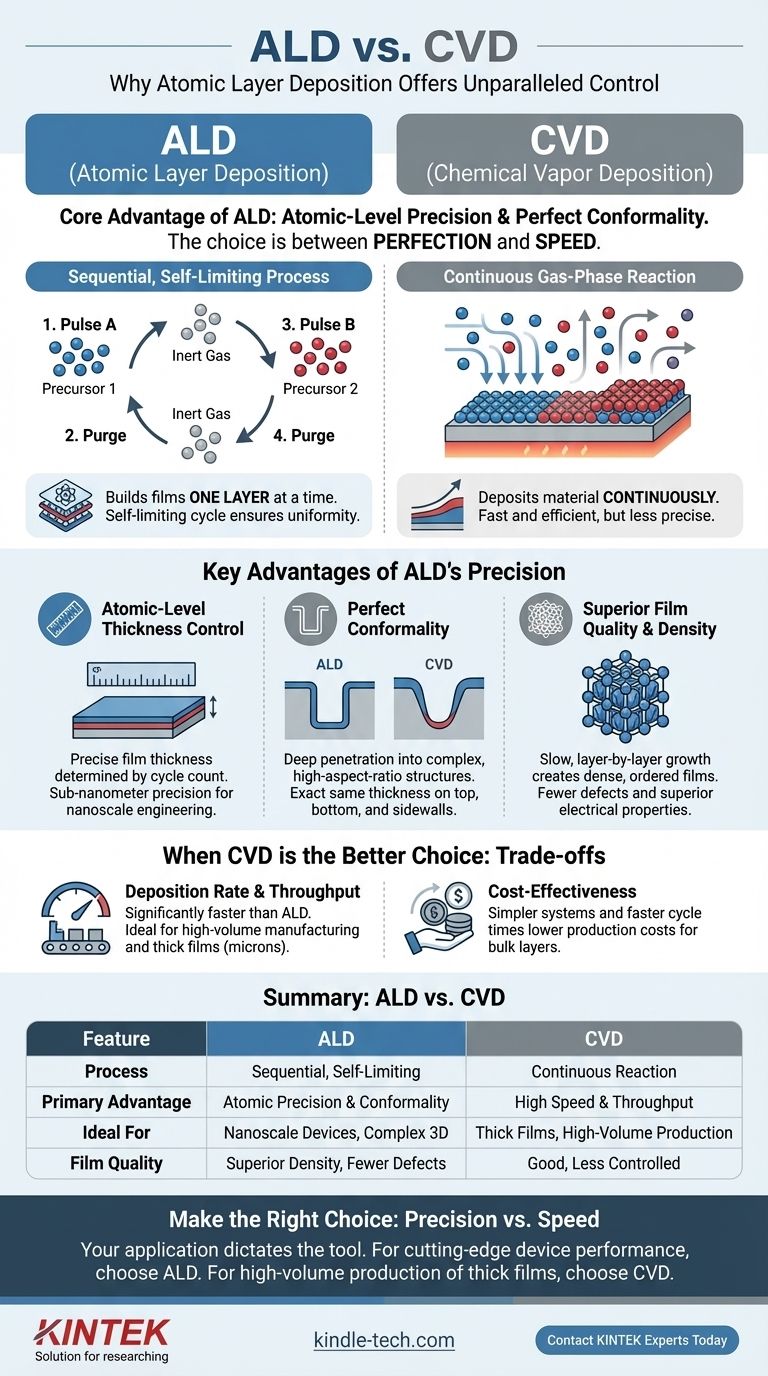
At its core, the primary advantage of Atomic Layer Deposition (ALD) over Chemical Vapor Deposition (CVD) is its unparalleled control. While both are methods for depositing thin films from gas-phase chemicals, ALD achieves atomic-level precision in film thickness and exceptional uniformity on complex 3D structures. This makes it the superior choice for cutting-edge applications requiring ultra-thin, perfect films, whereas CVD is engineered for deposition speed and efficiency on simpler surfaces.
The choice between ALD and CVD is a classic engineering trade-off between perfection and speed. ALD offers atomic-scale precision by building films one layer at a time, while CVD delivers production-level throughput by depositing material continuously.
The Fundamental Difference: Process Mechanism
To understand the advantages of ALD, you must first understand how its core mechanism differs from that of CVD. The process itself is the source of all its benefits.
CVD: A Continuous Reaction
In Chemical Vapor Deposition (CVD), one or more chemical precursors are introduced into a reaction chamber simultaneously.
These gases react together and on the heated substrate surface, leading to a continuous deposition of the desired material. This process is fast and efficient but can be difficult to control precisely.
ALD: A Sequential, Self-Limiting Process
Atomic Layer Deposition breaks the reaction into two distinct, sequential half-reactions, separated by purge steps.
- Pulse A: The first precursor gas is pulsed into the chamber. It reacts with the substrate surface until every available reaction site is occupied.
- Purge: Excess precursor gas and byproducts are purged from the chamber with an inert gas.
- Pulse B: The second precursor gas is introduced. It reacts with the layer formed by the first precursor.
- Purge: The chamber is purged again, completing one full ALD cycle.
This cycle is self-limiting. The reaction naturally stops after a single, uniform monolayer is formed. This is the fundamental source of ALD's precision.
Key Advantages of ALD's Precision
The unique, self-limiting mechanism of ALD gives rise to several powerful advantages for demanding applications.
Atomic-Level Thickness Control
Because each ALD cycle deposits a predictable and consistent amount of material (typically a fraction of a monolayer), the final film thickness is determined simply by the number of cycles performed.
This allows for the deposition of films with sub-nanometer precision, which is critical for modern semiconductor devices and nanoscale engineering.
Perfect Conformality
ALD's gas-phase precursors can penetrate deep into complex, high-aspect-ratio structures like trenches or pores.
The self-limiting nature of the reaction ensures that the film grows with the exact same thickness on the top, bottom, and sidewalls of these features. CVD struggles to achieve this, often resulting in thicker films at the opening and thinner films at the bottom.
Superior Film Quality and Density
The slow, layer-by-layer growth process allows atoms to arrange themselves into a highly dense and ordered structure.
This typically results in films with fewer defects, lower impurity levels, and superior electrical and mechanical properties compared to films deposited by the faster, less-controlled CVD process.
Understanding the Trade-offs: When CVD is the Better Choice
ALD's precision comes at a cost, and it is not the ideal solution for every problem. CVD remains a dominant technique for valid reasons.
The Need for Speed: Deposition Rate
The single greatest drawback of ALD is its slow deposition rate. Building a film one atomic layer at a time is inherently time-consuming.
For applications requiring thick films (many nanometers to microns), CVD is orders of magnitude faster and therefore more economically viable.
Throughput and Cost
CVD systems are often simpler and better suited for high-volume manufacturing where absolute perfection is not the primary requirement. The faster cycle time translates directly to higher wafer throughput.
For protective coatings, optical films, or other applications where thickness is measured in microns, ALD is often too slow to be practical.
Precursor Availability
As a more mature and widely used technology, CVD has a broader library of well-characterized precursors for a vast range of materials. While the library for ALD is growing rapidly, CVD often provides a more established starting point for depositing less-common materials.
Making the Right Choice for Your Goal
Your decision must be driven by the technical requirements and economic constraints of your specific application.
- If your primary focus is cutting-edge device performance: Choose ALD for its precise thickness control and unmatched conformality, which are essential for nanoscale transistors and high-aspect-ratio memory devices.
- If your primary focus is high-volume production or thick films: Choose CVD for its superior deposition rate and cost-effectiveness, making it ideal for industrial coatings, barriers, or bulk material layers.
- If your primary focus is pinhole-free film quality on a complex 3D structure: Choose ALD, as its self-limiting nature guarantees the uniform, dense coverage that CVD cannot easily replicate.
Ultimately, understanding the fundamental process difference—sequential precision versus continuous speed—empowers you to select the right tool for the job.
Summary Table:
| Feature | ALD (Atomic Layer Deposition) | CVD (Chemical Vapor Deposition) |
|---|---|---|
| Process Type | Sequential, self-limiting half-reactions | Continuous gas-phase reaction |
| Primary Advantage | Atomic-level precision & perfect conformality | High deposition speed & throughput |
| Ideal For | Nanoscale devices, complex 3D structures | Thick films, high-volume production |
| Film Quality | Superior density, fewer defects | Good, but less controlled |
Ready to Achieve Atomic-Level Precision in Your Lab?
Choosing the right deposition technique is critical for your research or production. KINTEK specializes in providing advanced lab equipment, including ALD and CVD systems, to meet your specific thin-film needs. Whether you require the unparalleled precision of ALD for cutting-edge semiconductor work or the high-throughput capabilities of CVD for industrial coatings, our experts can help you select the perfect solution.
Contact us today to discuss how our equipment can enhance your processes and deliver the high-quality results you demand.
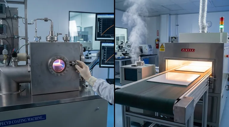
Visual Guide
Related Products
- Chemical Vapor Deposition CVD Equipment System Chamber Slide PECVD Tube Furnace with Liquid Gasifier PECVD Machine
- RF PECVD System Radio Frequency Plasma-Enhanced Chemical Vapor Deposition RF PECVD
- Electron Beam Evaporation Coating Oxygen-Free Copper Crucible and Evaporation Boat
- Hemispherical Bottom Tungsten Molybdenum Evaporation Boat
- Custom CVD Diamond Coating for Lab Applications
People Also Ask
- What are the advantages of chemical vapor deposition? Achieve Superior Thin Films for Your Lab
- What are the core advantages of PE-CVD in OLED encapsulation? Protect Sensitive Layers with Low-Temp Film Deposition
- Why is Chemical Vapor Deposition (CVD) equipment uniquely suited for constructing hierarchical superhydrophobic structures?
- What is the chemical vapor deposition growth process? Build Superior Thin Films from the Atom Up
- What types of substrates are used in CVD to facilitate graphene films? Optimize Graphene Growth with the Right Catalyst


