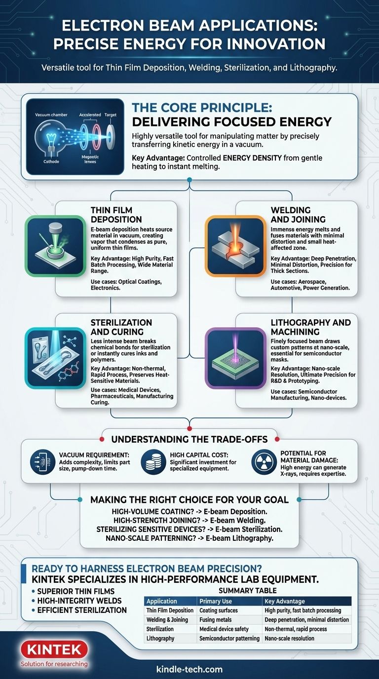
At its core, an electron beam is a highly versatile tool for precisely delivering energy. Its primary applications span multiple industries, including materials science for creating thin film coatings (deposition), advanced manufacturing for high-strength welding, medical device sterilization, and semiconductor fabrication for high-resolution lithography. The specific application is determined simply by how much energy is delivered and what material it is focused on.
While its applications seem vastly different—from coating a surface to sterilizing a syringe—they all derive from one fundamental principle: an electron beam is an exceptionally controllable method for transferring kinetic energy to a target material within a vacuum. Understanding this principle is the key to choosing the right application for your goal.
The Core Principle: Delivering Focused Energy
An electron beam is more than just a stream of particles; it's a tool for manipulating matter at a molecular level. Its capabilities stem from the precise control over this energy transfer.
How an Electron Beam Works
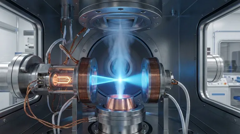
In simple terms, a high voltage is used to accelerate electrons emitted from a heated filament (cathode) toward a target (anode). This entire process occurs within a vacuum chamber to prevent the electrons from scattering off air molecules. Magnetic lenses then focus and steer this beam onto a target with incredible precision.
Precision and Control
The key advantage of an electron beam is the ability to control its energy density—the amount of energy concentrated in a specific spot. A low-energy, wide beam can gently heat a surface for coating, while a high-energy, tightly focused beam can vaporize or melt metal for welding or machining.
Key Industrial Applications
The ability to finely tune the beam's energy and spot size gives rise to its wide range of uses. Each application simply adjusts these parameters to achieve a different physical effect.
Thin Film Deposition
This process, often called E-beam deposition, uses a focused electron beam to heat and evaporate a source material (like a metal or ceramic) in a vacuum. The resulting vapor then condenses onto a substrate, forming an exceptionally pure and uniform thin film or coating.
As noted in materials science, it is often faster and more flexible for batch processing than alternatives like magnetron sputtering. It also allows for the use of a wider array of less expensive evaporative materials, making it ideal for high-volume commercial applications like optical coatings and electronics.
Welding and Joining
By concentrating immense energy into a tiny spot, an electron beam can instantly melt and fuse materials. This produces deep, narrow welds with minimal distortion and an extremely small heat-affected zone compared to conventional welding methods. This precision is critical in aerospace, automotive, and power generation industries for joining thick or dissimilar metals.
Sterilization and Curing
A less intense but broader beam can be used to break chemical bonds. In the medical field, this is used to sterilize packaged medical devices and pharmaceuticals without using high heat that could damage them. In manufacturing, it is used for cross-linking polymers or instantly curing inks and coatings, a process that is much faster than thermal or UV curing.
Lithography and Machining
At the highest end of precision, electron beam lithography (EBL) uses a finely focused beam to draw custom patterns on a surface coated with an electron-sensitive resist. This technique is fundamental to creating the masks used in semiconductor manufacturing and for prototyping nano-scale devices, offering resolution far beyond what is possible with light-based methods.
Understanding the Trade-offs
While powerful, electron beam technology is not a universal solution. Its unique requirements introduce specific limitations that must be considered.
The Vacuum Requirement
The most significant operational hurdle is the need for a vacuum. This necessitates a sealed chamber, which increases equipment complexity, limits the size of the part that can be processed, and introduces pump-down time into the workflow, potentially creating a bottleneck.
High Capital Cost
Electron beam systems, with their high-voltage power supplies, vacuum chambers, and magnetic optics, represent a significant capital investment. The cost is often higher than for competing technologies, making it best suited for applications where its unique benefits provide a clear return on investment.
Potential for Material Damage
The same high energy that makes E-beams useful can also be a liability. The beam can generate X-rays upon impact with the material, which may damage sensitive electronic components or substrates. Inexperienced operation can also lead to unwanted melting or vaporization of the target.
Making the Right Choice for Your Goal
To determine if an electron beam is the right tool, you must match its specific strengths to your primary objective.
- If your primary focus is high-volume, cost-effective coating: E-beam deposition is a strong candidate due to its speed in batch scenarios and its compatibility with a wide range of materials.
- If your primary focus is high-strength, low-distortion joining: E-beam welding offers unparalleled precision for thick sections or sensitive alloys where minimal heat input is critical.
- If your primary focus is sterilizing heat-sensitive devices: E-beam sterilization is an established, rapid, and effective non-thermal method that preserves material integrity.
- If your primary focus is creating patterns at the nano-scale: E-beam lithography provides the ultimate resolution for R&D and mask production, though it is slower for mass production.
Ultimately, harnessing the power of an electron beam comes down to understanding that you are not just choosing an application, but a precise method of energy delivery.
Summary Table:
| Application | Primary Use | Key Advantage |
|---|---|---|
| Thin Film Deposition | Coating surfaces | High purity, fast batch processing |
| Welding & Joining | Fusing metals | Deep penetration, minimal distortion |
| Sterilization | Medical device safety | Non-thermal, rapid process |
| Lithography | Semiconductor patterning | Nano-scale resolution |
Ready to harness the precision of electron beam technology for your lab?
At KINTEK, we specialize in providing high-performance lab equipment, including electron beam systems for deposition, welding, and more. Our solutions are designed to deliver the exact control and reliability your research or production demands.
Let us help you achieve:
- Superior thin films with our deposition systems.
- High-integrity welds for critical components.
- Efficient sterilization of sensitive materials.
Contact our experts today to discuss your specific application and find the perfect electron beam solution for your laboratory needs.
Contact KINTEK now for a personalized consultation!
Visual Guide
Related Products
- Electron Beam Evaporation Coating Tungsten Crucible and Molybdenum Crucible for High Temperature Applications
- Electron Beam Evaporation Coating Oxygen-Free Copper Crucible and Evaporation Boat
- E Beam Crucibles Electron Gun Beam Crucible for Evaporation
- Electron Beam Evaporation Coating Gold Plating Tungsten Molybdenum Crucible for Evaporation
- Electron Beam Evaporation Coating Conductive Boron Nitride Crucible BN Crucible
People Also Ask
- What is e-beam evaporation used for? Precision Coating for Optics, Aerospace & Electronics
- What are the applications of e-beam evaporation? Achieve High-Purity Coatings for Optics & Electronics
- What is e-beam evaporation? Achieve High-Purity Thin Film Deposition for Your Lab
- What materials are used in electron beam evaporation? Master High-Purity Thin Film Deposition
- What is the deposition rate of e-beam evaporation? Control Thin Film Quality and Speed


