At its core, Metal Organic Chemical Vapor Deposition (MOCVD) is the foundational manufacturing process for most modern LEDs, semiconductor lasers, and high-frequency power electronics. Also known as Metal Organic Vapor Phase Epitaxy (MOVPE), this technique is used to fabricate a wide range of devices including advanced transistors, solar panels, and other critical optoelectronic components made from compound semiconductors like Gallium Nitride (GaN).
MOCVD is not merely a coating technique; it is an atomic-scale construction method. Its true value lies in its ability to build complex, high-purity crystalline material layers with precise control, which is the fundamental requirement for high-performance electronic and photonic devices.
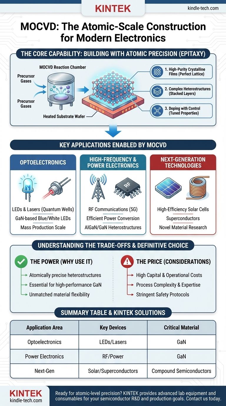
The Core Capability: Building with Atomic Precision
To understand the applications of MOCVD, you must first understand its fundamental capability: epitaxy. This is the process of growing a thin, single-crystal layer on top of a crystalline substrate. MOCVD excels at this with unmatched precision.
Growing High-Purity Crystalline Films
MOCVD works by introducing precise quantities of precursor gases (the "metal organics") into a reaction chamber containing a heated substrate wafer. The gases decompose at the hot surface, and the desired atoms arrange themselves into a perfect crystal lattice, continuing the structure of the substrate below. This results in films of exceptionally high purity and quality.
Creating Complex Heterostructures
The real power of MOCVD is its ability to rapidly switch between different gas sources. This allows engineers to grow a stack of different semiconductor materials on top of one another, each with a different composition. These stacks, called heterostructures, are the basis for most advanced devices. The transitions between these layers are atomically sharp.
Doping with Unmatched Control
Semiconductor function depends on intentionally introducing impurities, a process called doping. MOCVD allows for the introduction of dopant gases with extreme precision during the growth process, giving engineers fine-tuned control over the material's electrical properties.
Key Applications Enabled by MOCVD
MOCVD's ability to build these complex, high-purity structures directly enables the function of many modern technologies.
Optoelectronics: LEDs and Lasers
This is the most widespread application of MOCVD. To create light efficiently, LEDs and laser diodes require a structure called a quantum well, which consists of an ultra-thin layer of one material sandwiched between two layers of another. MOCVD is the only technology capable of producing these complex stacks with the uniformity and scale required for mass production, especially for GaN-based blue and white LEDs.
High-Frequency and Power Electronics
High-frequency devices for RF communications (like in 5G base stations) and high-power transistors for efficient power conversion rely on materials like Gallium Nitride (GaN). These devices use a specific heterostructure (e.g., AlGaN/GaN) to create a highly mobile channel of electrons. MOCVD is the essential tool for manufacturing these high-speed, high-power components.
Next-Generation Technologies
MOCVD is a versatile platform used to fabricate a wide range of other advanced materials. This includes high-efficiency multi-junction solar cells, which use multiple layers to capture different wavelengths of sunlight, and thin films for research into superconductors and other advanced electronic materials.
Understanding the Trade-offs
While powerful, MOCVD is a complex and resource-intensive technology. Its use implies a specific set of engineering and business priorities.
High Capital and Operational Costs
MOCVD reactors are sophisticated and expensive machines that require significant investment. They operate under precise conditions of temperature and pressure and demand extensive facility support, making the barrier to entry high.
Process Complexity and Expertise
Developing a stable, high-yield MOCVD process for a specific device is a significant R&D effort. It requires deep expertise in chemistry, material science, and physics to tune the dozens of process parameters for optimal results.
Precursor Chemistry and Safety
The "metal organic" precursors are highly reactive and often toxic or pyrophoric (ignite spontaneously in air). While modern liquid precursors are safer than older compounds, managing them still requires stringent safety protocols and specialized handling systems.
When is MOCVD the Definitive Choice?
The decision to use MOCVD is driven by the non-negotiable need for atomically precise, crystalline heterostructures.
- If your primary focus is mass-producing high-efficiency LEDs or laser diodes: MOCVD is the non-negotiable industry standard, as it is the only viable method for creating the required quantum well structures at scale.
- If your primary focus is fabricating high-frequency or high-power GaN transistors: MOCVD is essential for its precise control over the complex, multi-layered heterostructures that define device performance and reliability.
- If your primary focus is researching novel semiconductor materials or device structures: MOCVD offers unmatched material flexibility and atomic-level control, making it a critical tool for pushing the boundaries of material science and electronics.
Ultimately, MOCVD is chosen when the performance of the final device depends entirely on the perfection of its underlying crystal structure.
Summary Table:
| Application Area | Key Devices Produced | Critical Material (Example) |
|---|---|---|
| Optoelectronics | LEDs, Laser Diodes | Gallium Nitride (GaN) |
| High-Frequency/Power Electronics | RF Transistors, Power Converters | Gallium Nitride (GaN) |
| Next-Generation Tech | Multi-Junction Solar Cells, Superconductors | Compound Semiconductors |
Ready to integrate MOCVD technology into your laboratory's capabilities? KINTEK specializes in providing the advanced lab equipment and consumables necessary for cutting-edge semiconductor and materials research. Whether you are developing next-generation LEDs, high-power electronics, or novel materials, our expertise can support your R&D and production goals. Contact our team today to discuss how we can help you achieve atomic-level precision in your work.
Visual Guide
Related Products
- Multi Heating Zones CVD Tube Furnace Machine Chemical Vapor Deposition Chamber System Equipment
- 915MHz MPCVD Diamond Machine Microwave Plasma Chemical Vapor Deposition System Reactor
- Microwave Plasma Chemical Vapor Deposition MPCVD Machine System Reactor for Lab and Diamond Growth
- Cylindrical Resonator MPCVD Machine System Reactor for Microwave Plasma Chemical Vapor Deposition and Lab Diamond Growth
- Molybdenum Vacuum Heat Treat Furnace
People Also Ask
- What is the function of a high-temperature CVD tube furnace in 3D graphene foam prep? Master 3D Nanomaterial Growth
- What are the advantages of a multi-zone tube furnace for Sb2S3? Unlock Superior Semiconductor Thin Film Purity
- What are the advantages of using a Multi-zone Tube Furnace? Enhanced Thermal Uniformity for Diffusion Research
- What advantages do CVD furnaces offer for Wf/W composites? Preserving Fiber Ductility and Interface Integrity
- What is a CVD tube furnace? A Complete Guide to Thin-Film Deposition