At its core, thin film deposition is used across countless industries to give a base material surface properties it does not naturally possess. This technology is fundamental to modern electronics, medical devices, optics, and aerospace, enabling the creation of everything from semiconductor chips and LED displays to biocompatible implants and wear-resistant coatings.
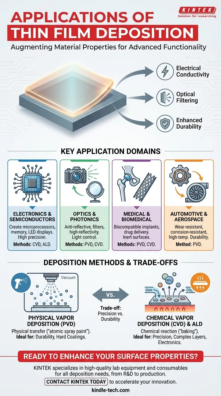
The true purpose of thin film deposition is not simply to add a layer, but to fundamentally transform a material's surface, granting it new capabilities such as electrical conductivity, optical filtering, or enhanced durability.
The Core Principle: Augmenting Material Properties
Thin film deposition is a foundational process in advanced manufacturing. It involves applying a layer of material, often just a few nanometers to micrometers thick, onto a substrate.
The Goal is Added Functionality
The primary driver for using this technology is to add essential properties. A bulk material, like glass or a metal alloy, might be strong or cheap, but it may lack the required electrical, optical, or chemical characteristics for a specific application.
Thin films solve this by creating a composite material where the substrate provides the structure and the film provides the specialized surface function.
Enabling Efficiency and Innovation
This process allows for the conservation of scarce or expensive materials by using only a microscopic amount where it is needed most—on the surface.
Furthermore, thin film deposition has enabled the creation of entirely new products and solutions to previously unsolved engineering challenges, particularly in the realm of nano-structured coatings and semiconductor devices.
Key Application Domains
The versatility of thin film deposition is best understood by looking at its impact across major technological sectors.
Electronics and Semiconductors
This is the most common and critical application. The semiconductor industry relies heavily on deposition to build the intricate, layered structures of microprocessors, memory chips, and other integrated circuits.
Techniques like Chemical Vapor Deposition (CVD) offer the atomic-level precision required to create the transistors and pathways that make modern electronics possible. It is also essential for manufacturing LED displays, semiconductor lasers, and consumer electronics.
Optics and Photonics
Thin films are used to precisely control how light interacts with a surface. This includes creating anti-reflective coatings for eyeglasses and camera lenses, high-reflectivity coatings for mirrors, and specialized optical filters that only allow specific wavelengths of light to pass through.
Medical and Biomedical Devices
In the medical field, biocompatibility is paramount. Thin films are deposited onto implants, such as artificial joints or stents, to create an inert surface that the body will not reject.
These coatings can also be engineered to provide other benefits, such as drug-delivery capabilities or antimicrobial properties, significantly improving patient outcomes.
Automotive and Aerospace
In industries where components face extreme conditions, durability is key. Thin films provide hard, wear-resistant coatings for cutting tools, engine parts, and landing gear.
These coatings dramatically increase the lifespan and performance of components by protecting them from friction, corrosion, and high temperatures.
Understanding the Methods and Trade-offs
The choice of deposition method is critical and depends entirely on the desired properties of the film and the substrate material. The two most dominant families of techniques are Physical and Chemical Vapor Deposition.
Physical Vapor Deposition (PVD)
PVD techniques, like sputtering or evaporation, involve physically transferring a material from a source to the substrate within a vacuum. Think of it as a highly controlled, atomic-level spray painting process.
PVD is excellent for depositing materials with high melting points and for creating very dense, durable, and hard coatings. This makes it ideal for tools and mechanical components.
Chemical Vapor Deposition (CVD)
CVD involves introducing reactive gases into a chamber, where they react on the surface of the substrate to form the desired film. It's more like baking, where the ingredients combine under heat to create a new solid layer.
CVD and its variant, Atomic Layer Deposition (ALD), offer exceptional conformity and atomic-level precision. This is why CVD is the dominant method in the semiconductor industry, where building flawless, complex layers is essential.
Choosing the Right Method
There is no single "best" method; there is only the right method for the application. The decision involves a trade-off between the required precision, the material being deposited, and the desired physical properties like hardness or purity.
High-precision electronic applications lean heavily on CVD, while applications requiring mechanical toughness often rely on PVD.
Applying This to Your Goal
Your choice of technology or material will be guided by the primary function you need the surface to perform.
- If your primary focus is high-precision electronics: You will almost certainly be working with films created by CVD or ALD for their unparalleled atomic-level control.
- If your primary focus is mechanical durability: PVD is often the more practical and robust choice for creating hard, wear-resistant coatings on tools, engines, or industrial components.
- If your primary focus is biocompatibility or optical performance: The choice between PVD and CVD will depend on the specific material required for the coating and the geometry of the substrate.
Thin film deposition is the invisible technology that empowers much of the modern world, proving that the most impactful changes often happen on the smallest of scales.
Summary Table:
| Application Domain | Key Function of Thin Film | Common Deposition Methods |
|---|---|---|
| Electronics & Semiconductors | Create microprocessors, memory chips, LED displays | Chemical Vapor Deposition (CVD), Atomic Layer Deposition (ALD) |
| Optics & Photonics | Anti-reflective coatings, optical filters, high-reflectivity mirrors | Physical Vapor Deposition (PVD), CVD |
| Medical & Biomedical Devices | Biocompatible surfaces, drug-delivery coatings, antimicrobial properties | PVD, CVD |
| Automotive & Aerospace | Wear-resistant, corrosion-resistant, high-temperature coatings | Physical Vapor Deposition (PVD) |
Ready to enhance your product's surface properties?
Whether you are developing cutting-edge semiconductors, durable aerospace components, or life-saving medical implants, the right thin film deposition process is critical to your success. KINTEK specializes in providing high-quality lab equipment and consumables for all your deposition needs, from research and development to full-scale production.
Let our experts help you select the perfect solution to achieve the precise electrical, optical, or mechanical properties your project demands.
Contact KINTEK today to discuss your specific application and discover how our expertise can accelerate your innovation.
Visual Guide
Related Products
- Aluminized Ceramic Evaporation Boat for Thin Film Deposition
- Tungsten Evaporation Boat for Thin Film Deposition
- Electron Beam Evaporation Coating Oxygen-Free Copper Crucible and Evaporation Boat
- Molybdenum Tungsten Tantalum Evaporation Boat for High Temperature Applications
- Vacuum Hot Press Furnace Machine for Lamination and Heating
People Also Ask
- What are thin films deposited by evaporation? A Guide to High-Purity Coating
- Why is an alumina boat selected for catalyst precursors? Ensure Sample Purity at 1000 °C
- Why is an alumina boat and Ti3AlC2 powder bed necessary for Ti2AlC sintering? Protect MAX Phase Purity
- What is the chemical method for thin film deposition? Build Films from the Molecular Level Up
- What are the applications of thin films deposition? Unlock New Possibilities for Your Materials


