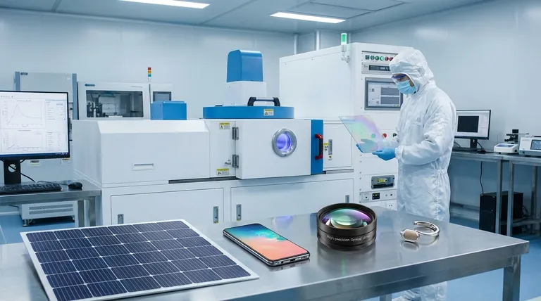
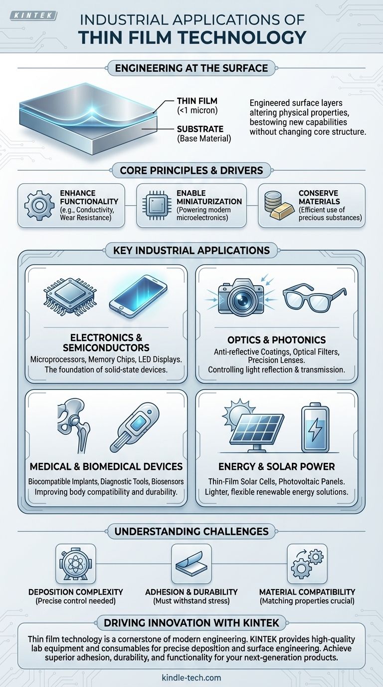
In industry, thin films are the foundational technology enabling everything from the screen on your smartphone and the processor in your laptop to advanced medical implants and high-efficiency solar panels. These engineered surface layers, often less than a micron thick, are applied to a base material (or substrate) to fundamentally alter its physical properties. This process allows engineers to bestow new capabilities upon a product without changing its core structure.
The central value of thin films lies in their ability to add powerful new functions—such as electrical conductivity, optical filtering, or wear resistance—to a material's surface. This enhances performance and creates new possibilities while conserving resources and enabling miniaturization.
The Core Principle: Engineering at the Surface
The primary reason thin films are so ubiquitous is that they separate a product's bulk properties from its surface properties. This allows for an optimized and efficient design where a low-cost, structurally sound material can be coated with a thin layer of another material that provides a specific, high-value function.
Enhancing Functionality
A thin film can add a property that the underlying material completely lacks. For example, a non-conductive piece of glass can be coated with a transparent conductive oxide to create a touch screen.
This principle is used to add wear resistance to cutting tools, reduce friction on moving parts, or control the reflection and transmission of light on optical lenses.
Enabling Miniaturization
The entire field of microelectronics is built upon thin film technology. By depositing, patterning, and etching incredibly thin layers of conductive, insulating, and semiconducting materials, we can create the microscopic integrated circuits that power all modern electronics.
Conserving Scarce or Expensive Materials
Many high-performance materials are either rare or expensive. Thin film deposition allows a minuscule amount of a precious material, like gold or platinum, to be applied over a much cheaper substrate, providing the desired surface property without the prohibitive cost of a bulk component.
Key Industrial Applications by Sector
The versatility of thin film deposition has made it an essential process in nearly every advanced industry. Its applications are diverse, touching consumer goods, scientific instruments, and critical infrastructure.
Electronics and Semiconductors
This is the largest and most well-known application area. Thin films are the building blocks of all solid-state devices.
Applications include the fabrication of integrated circuits, microprocessors, LED displays, and semiconductor lasers. The screen on your phone, tablet, and laptop relies on multiple layers of thin films to function.
Optics and Photonics
Thin film coatings are critical for controlling light. By applying layers with specific thicknesses and refractive indices, engineers can precisely manage how light is reflected, transmitted, or filtered.
This is essential for precision optics in cameras and telescopes, anti-reflective coatings on eyeglasses, optical filters used in scientific instruments, and fiber lasers.
Medical and Biomedical Devices
In medicine, surface properties are critical for ensuring a device is compatible with the human body and functions as intended.
Thin films create biocompatible coatings on medical implants like artificial joints and stents, preventing rejection and improving durability. They are also used to prepare specialized microscopy and microanalysis slides for diagnostics.
Energy and Solar Power
Thin films play a significant role in renewable energy. Thin-film solar cells are manufactured by depositing layers of photovoltaic material onto a substrate like glass or plastic.
This technology contributes to lighter, more flexible, and potentially less expensive solar panels compared to traditional crystalline silicon wafers.
Understanding the Challenges
While the benefits are immense, working with thin films is a highly specialized engineering discipline. The success of an application is not guaranteed and depends on overcoming key technical hurdles.
Deposition Complexity
Applying a perfectly uniform layer of material that may only be a few dozen atoms thick is an incredibly complex physical and chemical process. It requires sophisticated vacuum equipment and precise control over variables like temperature, pressure, and source material purity.
Adhesion and Durability
A thin film is only as good as its bond to the substrate. Ensuring the coating adheres properly and can withstand mechanical stress, thermal cycling, and environmental exposure is a primary challenge. A poorly adhered film can flake or delaminate, causing total device failure.
Material Compatibility
The chemical, thermal, and mechanical properties of the film and the substrate must be compatible. A mismatch in the rate of thermal expansion, for example, can cause the film to crack or peel as the device heats and cools during operation.
How Thin Films Drive Your Goal
The decision to use thin film technology is directly tied to the specific performance you need to achieve.
- If your primary focus is creating advanced electronics: Thin films are the non-negotiable building blocks for fabricating microprocessors, memory chips, and displays.
- If your primary focus is improving optical performance: Thin film coatings are the primary method for controlling light reflection, transmission, and filtering in lenses, sensors, and displays.
- If your primary focus is developing next-generation medical devices: Thin films provide the critical biocompatible and functional surfaces needed for implants, biosensors, and diagnostic tools.
- If your primary focus is enhancing material efficiency and reducing cost: Thin film deposition allows you to leverage the properties of expensive materials on cheaper substrates, unlocking performance that would otherwise be cost-prohibitive.
Ultimately, thin film technology is a cornerstone of modern engineering, allowing us to design and manufacture products that are smaller, more powerful, and more efficient than ever before.
Summary Table:
| Industry Sector | Key Thin Film Applications |
|---|---|
| Electronics & Semiconductors | Microprocessors, Memory Chips, LED Displays |
| Optics & Photonics | Anti-reflective Coatings, Optical Filters, Precision Lenses |
| Medical & Biomedical Devices | Biocompatible Implants, Diagnostic Tools, Biosensors |
| Energy & Solar Power | Thin-Film Solar Cells, Photovoltaic Panels |
Ready to enhance your product's performance with advanced thin film technology? KINTEK specializes in providing high-quality lab equipment and consumables for precise thin film deposition and surface engineering. Whether you're developing next-generation electronics, medical implants, or energy solutions, our expertise can help you achieve superior adhesion, durability, and functionality. Contact us today to discuss how we can support your laboratory's innovation goals!
Visual Guide
Related Products
- Aluminized Ceramic Evaporation Boat for Thin Film Deposition
- Tungsten Evaporation Boat for Thin Film Deposition
- Electron Beam Evaporation Coating Oxygen-Free Copper Crucible and Evaporation Boat
- Molybdenum Tungsten Tantalum Evaporation Boat for High Temperature Applications
- Aluminum-Plastic Flexible Packaging Film for Lithium Battery Packaging
People Also Ask
- Why is an alumina boat selected for catalyst precursors? Ensure Sample Purity at 1000 °C
- What is thin film deposition? Unlock Advanced Surface Engineering for Your Materials
- Why are high-purity ceramic boats used for lignin activation? Ensure Purity & Thermal Stability
- What are thin films deposited by evaporation? A Guide to High-Purity Coating
- What are the applications of thin films deposition? Unlock New Possibilities for Your Materials


