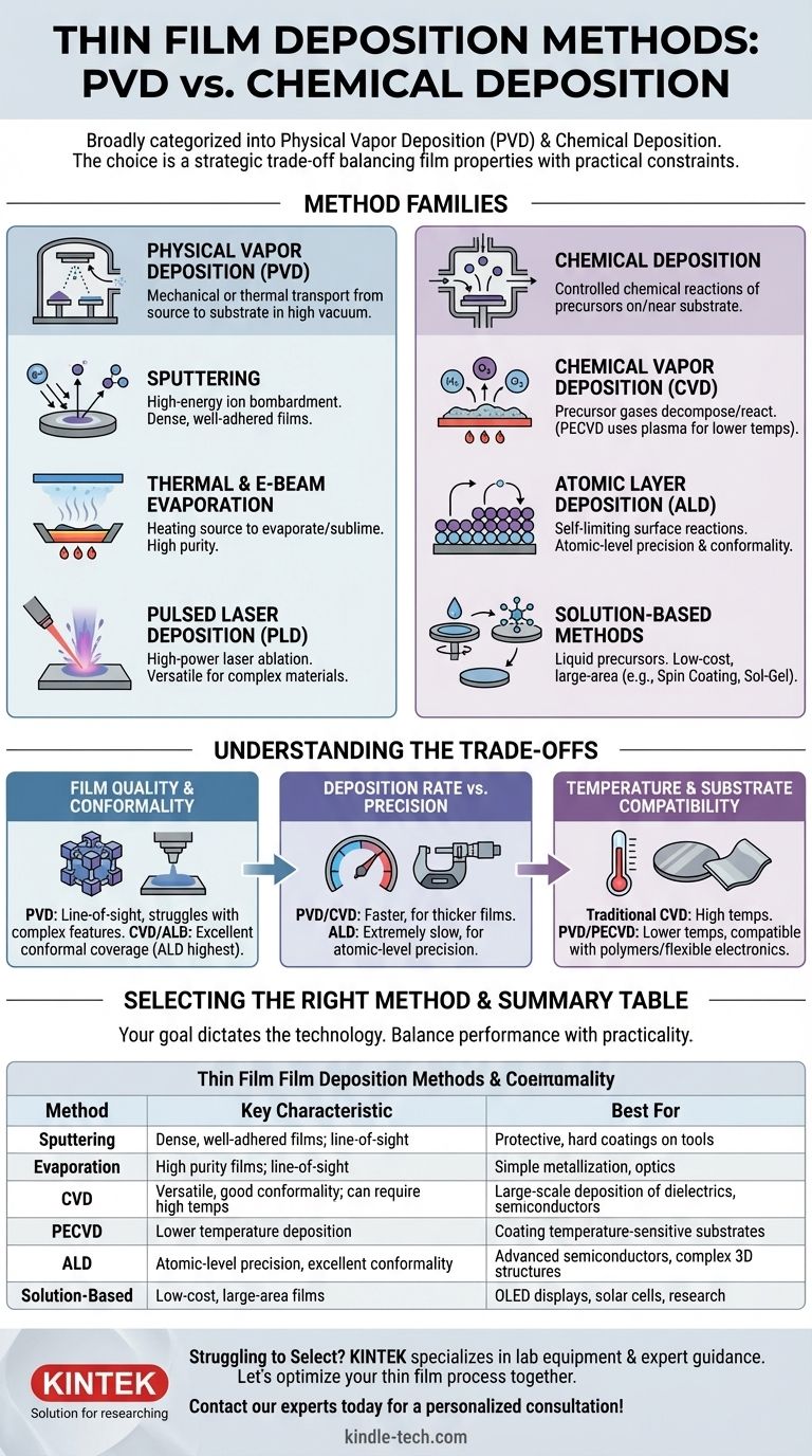
The primary methods for thin film deposition are broadly categorized into two families: Physical Vapor Deposition (PVD) and Chemical Deposition. In PVD, a source material is physically transferred—by being evaporated or sputtered—onto a substrate within a vacuum. In contrast, chemical methods use chemical reactions, often from precursor gases or solutions, to grow or form a film on the substrate’s surface. More advanced techniques like Atomic Layer Deposition (ALD) refine the chemical approach to build films with single-atom-layer precision.
The choice between deposition methods is not about finding the single "best" technique, but about making a strategic trade-off. Your decision must balance the required film properties—such as purity, density, and uniformity—against practical constraints like deposition speed, temperature sensitivity of the substrate, and overall cost.
Physical Deposition Methods: Transferring Material Atom by Atom
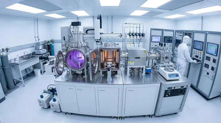
Physical deposition techniques involve the mechanical or thermal transport of material from a source to a substrate. These processes are almost always conducted in a high-vacuum environment to ensure the purity of the resulting film.
Sputtering
Sputtering is a process where a solid target of the desired material is bombarded with high-energy ions, typically from a plasma like argon. This energetic collision physically "knocks loose" atoms from the target, which then travel through the vacuum chamber and deposit onto the substrate, forming a thin film. It is renowned for producing dense, well-adhered films.
Thermal and E-beam Evaporation
This method involves heating a source material in a high vacuum until it evaporates (for liquids) or sublimes (for solids). The resulting vapor travels through the chamber and condenses on a cooler substrate. The heating can be done by passing a current through a resistive boat holding the material (thermal evaporation) or by using a focused high-energy electron beam (e-beam evaporation).
Pulsed Laser Deposition (PLD)
In PLD, a high-power pulsed laser is focused on a target within a vacuum chamber. The intense energy ablates the surface of the target, creating a plasma plume that expands and deposits onto the substrate. This technique is highly versatile for complex materials.
Chemical Deposition Methods: Building Films from Reactions
Chemical methods rely on controlled chemical reactions to create the thin film. The source materials, known as precursors, are introduced and react on or near the substrate surface.
Chemical Vapor Deposition (CVD)
CVD is a workhorse technique where precursor gases are introduced into a reaction chamber. These gases decompose or react on a heated substrate to form the desired solid film. A common variant, Plasma-Enhanced CVD (PECVD), uses a plasma to energize the precursor gases, allowing the deposition to occur at much lower temperatures.
Atomic Layer Deposition (ALD)
ALD is a specialized form of CVD that builds films one atomic layer at a time. It uses a sequence of self-limiting chemical reactions, where precursor gases are pulsed into the chamber one by one. This process offers unparalleled control over film thickness and produces exceptionally uniform and conformal films, even on highly complex 3D structures.
Solution-Based Methods (Sol-Gel, Spin Coating)
These methods involve applying a liquid precursor to a substrate. In spin coating, the substrate is spun at high speed to spread the liquid into a thin, uniform layer. In the sol-gel process, a chemical solution (the "sol") transitions into a gel-like phase on the substrate. Both typically require a subsequent heating step to remove solvents and solidify the final film.
Understanding the Trade-offs
Choosing the right method requires understanding its inherent advantages and limitations. The decision almost always comes down to balancing performance with practicality.
Film Quality and Conformality
PVD techniques are line-of-sight, meaning they struggle to coat the sides and bottoms of complex features. In contrast, CVD and especially ALD are non-line-of-sight and provide excellent conformal coverage, which is essential for modern microelectronics. ALD delivers the highest possible conformality and purity.
Deposition Rate vs. Precision
There is a direct trade-off between speed and control. PVD and CVD processes can deposit material relatively quickly, making them suitable for thicker films, such as protective tool coatings. ALD is extremely slow by comparison, but its atomic-level precision is non-negotiable for fabricating the most advanced semiconductor devices.
Temperature and Substrate Compatibility
Traditional CVD often requires very high temperatures to drive the necessary chemical reactions, which can damage sensitive substrates. PVD methods like sputtering and techniques like PECVD can operate at much lower temperatures, expanding the range of compatible materials, including polymers and flexible electronics.
Selecting the Right Method for Your Application
Your goal dictates the optimal technology. Use the following guidelines to narrow your choice:
- If your primary focus is protective, hard coatings on tools (e.g., Ti-Al-N): PVD methods like sputtering are the industry standard for their high film density and strong adhesion.
- If your primary focus is uniform, conformal films for advanced semiconductors: ALD is the definitive choice for its unmatched precision and ability to coat complex topographies.
- If your primary focus is depositing a wide range of materials, including dielectrics, on a large scale: CVD offers excellent versatility and throughput for applications not requiring atomic-level precision.
- If your primary focus is low-cost, large-area films for applications like OLED displays or solar cells: Solution-based methods like spin coating or spray pyrolysis can be highly effective and scalable.
Ultimately, the ideal deposition technique is a direct function of the material, the required film properties, and the underlying substrate, turning a complex choice into a clear engineering decision.
Summary Table:
| Method | Category | Key Characteristic | Best For |
|---|---|---|---|
| Sputtering | Physical Vapor Deposition (PVD) | Dense, well-adhered films; line-of-sight | Protective, hard coatings on tools |
| Evaporation | Physical Vapor Deposition (PVD) | High purity films; line-of-sight | Simple metallization, optics |
| CVD | Chemical Deposition | Versatile, good conformality; can require high temps | Large-scale deposition of dielectrics, semiconductors |
| PECVD | Chemical Deposition | Lower temperature deposition | Coating temperature-sensitive substrates |
| ALD | Chemical Deposition | Atomic-level precision, excellent conformality | Advanced semiconductors, complex 3D structures |
| Spin Coating / Sol-Gel | Solution-Based | Low-cost, large-area films | OLED displays, solar cells, research |
Struggling to Select the Right Deposition Method for Your Lab's Needs?
Choosing between PVD, CVD, and ALD is a critical decision that impacts your research quality, throughput, and budget. KINTEK specializes in lab equipment and consumables, serving laboratory needs with expert guidance.
We can help you navigate the trade-offs to identify the perfect technique for your specific application, whether you require the atomic-level precision of ALD for semiconductor research or the robust, high-density coatings from PVD for material science.
Let's optimize your thin film process together.
Contact our experts today for a personalized consultation!
Visual Guide
Related Products
- Aluminized Ceramic Evaporation Boat for Thin Film Deposition
- Tungsten Evaporation Boat for Thin Film Deposition
- Electron Beam Evaporation Coating Oxygen-Free Copper Crucible and Evaporation Boat
- Molybdenum Tungsten Tantalum Evaporation Boat for High Temperature Applications
- HFCVD Machine System Equipment for Drawing Die Nano-Diamond Coating
People Also Ask
- What are thin films deposited by evaporation? A Guide to High-Purity Coating
- What is thin film deposition? Unlock Advanced Surface Engineering for Your Materials
- What is the widely used boat made of in thermal evaporation? Choosing the Right Material for High-Purity Deposition
- Why are high-purity ceramic boats used for lignin activation? Ensure Purity & Thermal Stability
- Why is an alumina boat and Ti3AlC2 powder bed necessary for Ti2AlC sintering? Protect MAX Phase Purity


